Designing the RhoCoCo Retro Home COlor COmputer hardware
| Project RhoCoCo Retro HOme COlor COmputer | |
|---|---|
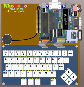
| |
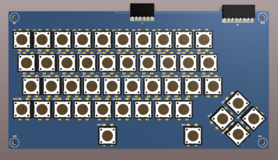
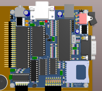
| A brand new 8-bit homecomputer with modern parts. Above picture is an artist impression, showing how it could look, mounted on a plank of wood measuring 20cm wide and 22 cm deep. An expansion board can be connected to the main board in the top left corner. Conceptually it resembles my earlier ZX81 clone but when finished it will be a capable Z80 based 128K full color home computer, able to drive a VGA monitor in high resolution, and with 64 colors, it has sound, and will have (BBC) BASIC and an SD-card for storage. | |
| Status | In progress |
| Contact | Mahjongg |
| Last Update | 2020-07-29 |
Less is more, less complexity, more fun is the driving force behind the Rhococo (Retro Home Color Computer).
This describes my desire, and the result of that desire, to build an 80's Home Computer in this decade (in the year 2017, 2018 and 2019). This first page describes what it took to design the hardware for RhoCoCo, planned future page will describe the design of an enclosure, and the firmware.
My long time desire (see this document File:My Home Computer intro.odt ) was to remake a home-computer inspired on, but not compatible with, the Sinclair spectrum and/or Amstrad CPC, Initially I considered not basing it on a Z80, but on an ARM7TDMI based simple micro-controller, (probably an STR710FZ2) running at 66MHz with 256 + 16 KB internal fast Flash and with 64K internal fast RAM and a separate external 32K VRAM. But early 2017 I changed my mind, because I wanted the ability to port software from various Z80 based homecomputers, of which there were many (many more than those using other processors, like the 6502, 6809, or 1802, to name a few). see how many there were: [1]
The idea behind it is to bringing back a new home computer, such as they were popular in the 80's, but build with modern components, and using modern interfaces (VGA monitor instead of TV, SD-card storage devices instead of cassette recorders).
I want it to be capable of at least a 320x200 VGA full high resolution graphics 16 color display (i.e. with Mode "D" timings, 70Hz, Horizontal Sync = 31.778 KHz, pixel clock 25.175 MHz).
To be able to keep the design simple, and thus cheap, but still able to be drive a VGA monitor, I pondered to support only the lowest VGA resolution of 320 x 200 with 16 colors. which means we only need to have, (and manipulate) a 256000 bit (32K) frame buffer. Three bytes could be shifted to the Red, Green an Blue color inputs, and one to the intensity input, giving sixteen colours per pixel. Preferably the "glue logic" for it will consist of standard logic, but if necessary I will consider a small FPGA (but rather not).
the Rhococo will support a simple SD-Card interface as storage, and will use a keyboard similar to my previous ZX81+34 design, but with more, and real, keys,and a more conventional keyboard imprint. This also means that rhococo will be just a bit larger than the Z81, so very small (and thus hopefully also very cheap). as a comparison think about the French "Alice" computer, or the small tandy MC-10. But much more capable than these two.
For sound I consider a PWM output. Or an emulated PSG (programmable sound generator). with at least similar capabilities to these used in the Amstrad CPC, spectrum + and MSX computers, but hopefully with capabilities not unlike a C64 SID chip.
It will be a "turn on and use" system, meaning that the "OS", and a programming language will permanently reside in ROM, ready the moment you turn the Rhococo on (Meaning it will be based on some kind of interpretative language), probably BASIC (if possible BBC BASIC).
It will not be yet another Linux based system, as I want something that can be completely understood, just like you could learn how any of the 80's homecomputers worked. It is deliberately a simple and limited system.
You can comment on it on the topic I started about it on the Raspberry PI forum, here: https://www.raspberrypi.org/forums/viewtopic.php?f=62&t=226889
April 18, 2017 Changed my mind, will try to build a Z80 based more "home computer like design"
Initially I wanted to build an ARM processor based design, this is what I wrote in 2015 on the subject (in Dutch) File:Rhococo Retro HOme COlor Computer design specs .odt. After a year or so contemplating this idea of a new homecomputer, I came to the conclusion that an ARM based system with software VGA generation might be too complex for a the simple system I had in mind. I will make a NEW homecomputer design with components that can be bought in 2017 (and hopefully the next few decades). It will be based on a Z80 compatible CPU as it is one of the few 8-bit CPU's that is still relatively easy to get, and it was so popular in the 80's that there is a plethora of software available for them. One thing I don't want is to use an FPGA for it, as these are still relatively expensive and difficult to program for. This does cause a problem, as most old homecomputers either used some kind of programmable logic (Sinclairs ULA logic) or were based around a CRTC like the MC6845, which are no longer available, or they used a VDC (video display controller) like the TMS9918 (MSX an many others) which are also no longer available. My preference would have been using a CRTC, but as I said I can find no CRTC's for sale anymore, I could build one with standard logic (like the TRS-80 did) but that's too RETRO even for me, (uses far too many components). Instead I'm wondering if I can replace the CRTC with an simple AT-mega (Arduino) microcomputer. For a 320 x 200 display you would need 320 / 8 = 40 8-pixel wide rows and 200 lines, which means you need 40 * 200 = 8000 address locations, this is about 8191 or 2 ^ 13, meaning you need 13 address lines to address these 8191 (or hex 0x1FFF) locations. and a couple of other signals like HSYNC and VSYNC and video clock. An Arduino (nano) uses an ATmega328, and doesn't really have that many GPO (output) ports, but that can be solved with a few 8-bit latches. I'm planning to do this in little steps, so first I'm planning to connect 8K Byte SRAM (or an EPROM for testing) to an Arduino nano, plus a shift register to clock out a video stream, to try to generate a 320 x 200 (monochrome) VGA signal, using a Arduino nano as a CRTC surrogate. Then continue from there.
April 23, 2017 Found some inspiration on what is possible with an ATMega328
I have looked (googled) a bit around if others had tried to combine a Z80 with an Arduino (ATMega328 chip which from now on I will call he AVR) and found this https://hackaday.io/project/19000-a-4-4ics-z80-homemade-computer-on-breadboard which isn't exactly what I want but seems to prove you can control a Z80 from an AVR, and do such things as catching I/O requests, and take over the Z80 bus to "fake" data being read from "ROM" (faked by the AVR) so you can feed some boot code to the Z80 which then uses I/O reads to get more data from the AVR to load in RAM. This is a nice idea, but you need quite some GPIO's to catch which address the Z80 reads from so you can feed it the right bytes. However, I considered that you can also completely take over the Z80's data and address busses, and use the AVR to load data into the RAM and use this method filling RAM with Z80 bootable content, (when adding an AVR controlled 16-bit counter for the address bus) then boot the Z80 from RAM. These ideas and others make that I can foresee that many other technical tricks can be pulled, like creating VGA color video this way. In any case I think that the ability to use the AVR as a virtual Z80 peripheral is very promising.
I also looked at other small Z80 systems, but they all are quite primitive IMHO or use things like bit banging to access I/O devices like serial ports, PS/2 keyboards and SD-cards, which is in my view a wrong approach as it uses Z80 CPU cycles too much, for things that a AVR could do more easily with virtual I/O.
The fact that you can use just a Z80, a 64K SRAM chip and an AVR chip to create a $4 CP/M capable machine is exhilarating, but I have set my goal on a color capable SBC that can be used with most (VGA) monitors, and has a built in keyboard, can run BASIC and has a clear architecture, and is cheap to reproduce.
For example I think it would be possible for the AVR to stop the Z80 (take over the bus) use the AVR to read some data from the RAM, then store it in the video shift register(s) one or more for each RGB and intensity shift register, and in this way create a 16 color video stream, you can use the very same 16-bit shift register you use for storing data in RAM for reading out sequential bytes from RAM to create video .
The very same AVR chip can also do many other things like creating PWM audio, (emulating a sound chip) reading keyboard data, and loading/storing files from an SD-card, and also creating a serial I/O channel, and I2C for I/O expansion, the possibilities seem endless. The bootable image data the system loads can be stored a simple serial EEPROM.
I think that the first thing I should do is to replicate the $4 4-chip homebrew computer, and experiment with it. This is its schematic: File:Z80 with AVR schematic.pdf
April 25 Started building up the prototype
Luckily RevSpace has breadboards, so I could start building the prototype. I thought the Hackaday design used the AVR chip used in the Arduino, the ATMega328, so I could replace it with an Arduino nano, but not so, it uses an ATMega32A, thankfully Bernadsky donated one to me, so I could start. He will also buy the 128K Byte SRAM 32-pin DIP chips for me from Farnell using the RevSpace account we have, that saves me from buying one through my work.
I have set up the breadboards, with the example from the pictures and video's of the Hackaday site. Added a Z80, an Atmega32A, and the 74HC00 and several buttons and LED's, capacitors and diodes, and connected up several GND, VCC and other connections. Next week I will continue. By then I will have made stickers for on the 3 main chips, so its easier to connect up buses and such. P.S. Stickers are ready. 26/4/2017.
Some thoughts about PAL versus other video output modes
I thought about creating PAL color video instead of VGA, there are "tech demo's" creating PAL color video, that means the AVR code also generates color-bursts, and phase shifted color information, using nothing but an AVR, but I don't think I can practically integrate such a design with my idea of using an AVR to read video data out of Z80 RAM-space, and also, at the same time, do virtual I/O handling, and sound generating.
Also these tech-demo's create a quite a low resolution video signal, which doesn't satisfy me.
So I think that is not the way to go. Problem is that the color encoders (Chips used to convert RGB or YUV data to composite color video) used in the Spectrum and later systems (such as LM1889 and MC1377 chips) are no longer sold. and RGB monitors are also gone the way of the Dodo. So for the moment keeping to the VGA video seems the only obvious solution.
So the basis should be that the AVR takes out video data from Z80 RAM and converts it to a pixel stream. Do do so, and to simplify filling that RAM from the AVR (while freeing up some much needed GPIO's) I suppose I need to implement an 8-bit counter, for the lowest 8-adress lines, complemented with an 8-bit latch for the highest 8-address lines, both with three state outputs to the address bus. So I can fill 256 sequential RAM locations from any of 256 address blocks, but also read 256 bytes out from video-ram into the AVR from any of the video RAM blocks, and one byte at the time keep feeding a video shift register with it, where the output of the video pixels go to a multiplexer so that 4-bit RGBY information is switched between a foreground and a background color. The two nibbles of which can be changed simultaneously with storing a byte in the video shift register.
For keyboard I/O I'm thinking of an 8x8 keyboard array accessed (Spectrum style) with a single 8-bit data-bus driver for the 8 columns, while 8-rows are driven from 8 address lines, and read out with a virtual I/O command at the end of a video screen cycle.
Also virtual I/O could be used to control a virtual programmable sound generator on the AVR which outputs sound on a PWM output of the AVR.
Using the RAM access shift register/latch combo can/should replace the 6 GPIO lines now used to store 512 bytes of boot code in RAM, and should free up a few GPIO lines, which are quite dire and we do need some.
Also we probably need code space which is now used to contain Z80 code, I suppose we could off-load the Z80 code to an external I2C/SPI EEPROM or possibly to an SD-Card (in a later stage). Which also makes using much larger Z80 images possible.
April 30, 2017 added most wiring, except for SRAM
The SRAM chip is unfortunately still missing, Benadski wasn't there so I couldn't ask him about it. Stickers were cut out, plasticized, and stuck on the Z80 and ATMega32A (but not on the missing SRAM chip) and wired with DuPont wires, using "resistor" color codes, like A0 = Black A1 = brown A2 = red etc. most wiring is done, its now waiting for the SRAM chip so I can finish wiring. After that I intend to in circuit program the ATMega32A. An USB serial device has also been added to the design.
May 2, 2017 added SRAM chip, finished wiring
Now I only need to double check the wiring, which is much more intense than I thought, seeing the pictures of the original, probably because I use DuPont wires. It doesn't seem very reliable. Now I have to figure out how to program the ATMega32A. First task is probably installing the latest Arduino IDE.
May 9, 2017 Programmed the ATMega32A and started testing
Installed the Arduino IDE, and found it didn't offer programming a bare ATMega32A. Found a source called "Mightycore" that offered programming options for ATmega32A's. Managed to get the programming code "S221116_Z80_Breadboard.ino" compiled after selecting the ATMega32, (had to remove the ATMega32A from the breadboard for programming) and managed to get the USBbus programmer working. Finally the code was uploaded to the Mega32A, and I saw a lot of code space was still free.
Installed a driver for the USB serial adapter, and got it to work, first with the built in monitor, later I installed PUTTY, and configured it for 9600 baud etc, and it worked... Partly.
I got all the messages from the ATMega running the code, upto the message:
"IOS: Z80 is running from now."
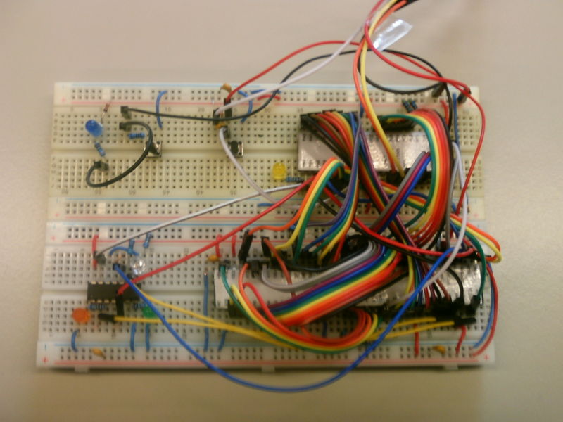
then, nothing.... :-( so the z80 uBIOS doesn't run, probably some wiring error still. Although it seems to finish running the first and second boot parts, with help from the Z80 for the second part. Next time debugging, and probably building it up on perfboard for better reliability and the possibility to remove the main chips from sockets, or even to add a programmer interface, for easier programming, although the ability to just take the ATMEGA32 out of its socket will also help a lot, as taking it out of the breadboard is now a pain, with all the Dupont wires crisscrossing over it. Here is a picture of it on breadboard.
As can be seen, its very hard to take out any parts, for example the ATMega32 for (re-)programming, and all these loose wires that loop through the air make for a noisy and unreliable system. So I will start putting it on a hand wired perfboard, at this stage designing a PCB isn't a good idea, as I will interactively, step by step, expand the design from the base design to a version that will be able to create a video signal. This will probably mean many intermediate steps and a hand wired perfboard is the easiest solution. I will also buy a programmer (a MINIPRO TL866) so I can easily program the ATMega32, and it will also service to program EPROM's and OTP's.
May 23, 2017 Started building perfboard version
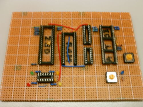
Took a piece of perfboard, and mounted two 40 pin sockets for Z80 and ATMega32 a 32 PIN socket for 128K SRAM, a 14 pin socket for the 74HC00, and added two 20 pin sockets in between ATMega32 and SRAM for future expansions I have in mind (one 8-bit latch with 3-state outputs between databus and upper 8 address lines (including A17), and one 74HCT590 8-bit counter with 3-state outputs for the lower 8 address lines). Also added all resistors, capacitors diodes and LED's, as well as the two buttons. Next time I will start the wiring, starting with the GND, and then +5V wiring. After that I will probably draw my own schematic, so I can also add wiring to the two 20 pin expansion sockets (although these won't be used yet at this stage).
June 6, 2017 drawn schematic of first version in KiCAD
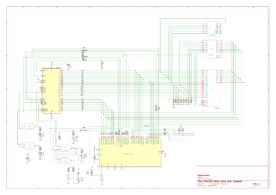
I decided that for this project I would switch from my old and beloved, Ultiboard to the new and more universally adapted KiCAD. So I installed KiCAD, and learned to use it. This is my own drawing in KiCAD of the "4 chip $4 Z80 computer" that will become the basis of RhOCoCo, its extended with (for the moment non functioning) address generation logic consisting of an 8-bit counter, and an 8-bit latch: File:RHOCOCO REV 1.1.pdf
The 8-bit latch for the higher 8 address lines, and the 8-bit counter for the lower 8 address lines will form the infra structure that will enable the ATMega32 access to all of the RAM for storing code into the RAM, and do Z80/ATMega32 memory sharing of video RAM later, also for memory mapped keyboard I/O (spectrum/TRS-80 style). In the first testing phase the data and address busses of the counter and latch will be wired up on the bread board, but won't be controlled, and the IC's will not be inserted into their sockets, so the same bootstrap method can still be used as the 4-chip $4 computer uses, later if the breadboard works, the address lines from the ATMega32 to the Z-80 bus will be removed, freeing up 9 GPIO pins for new functions (PC2 to PC7 and PD2 to PD4) and my own RAM access system will replace it, using a few of these GPIO's but still leaving some others for other uses. If that bootstrap system works I will add an 8-bit latch and video shift register to the data-bus so that a (monochrome) video stream can be generated, which can switch between a foreground and a background color using a dual 4-bit multiplexer. each 4-bits will come from another 8-bit latch. so in theory each 8 consecutive pixels can have either a foreground or a background color, the resulting 4-bit video data will generate sixteen foreground or background colours, as two levels each of R, G, and B signals. This color data will go to the VGA plug together with h-sync and v-sync data from the ATMega32.
June 14, 2017 added some ground wiring and stickers
Designed stickers for the 74HC590, and 74HC574 chips, in mirrored form to paste to the back of the bread board, replaced the 14-pin socket to a 16-pin socket for the 74HC590, and added GROUND and VCC wiring to the bread board. Next time I should bring some wire wrap wire for the wiring of address, data and control wires. It will be lots of work to wire this board up. Hopefully it will be worth it, and be much more reliable than the breadboard.
June 14 to July 12 wired up my prototype board
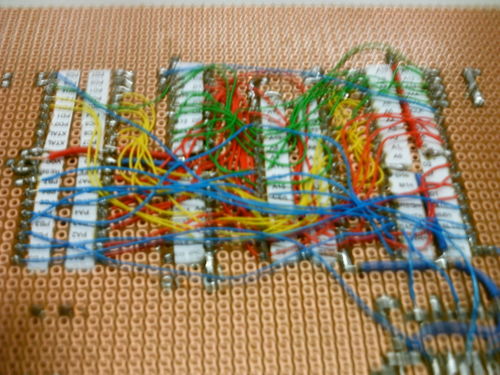
Well, I't took a long while, but I'm now nearly finished with wiring up my prototype board, here are a few (bad) pictures of the board so far, and the wiring on the back.
Colors of wires are:
Thick Red, +5V
Thick Blue, or uninsulated, GND
Red, Databus
Yellow, lower 8 address lines
Green, Higher 8 address lines
Blue, control signals
May 23, 2018, gave up the version with an ATMega, and switched to using a Parallax Propeller (P8X32A) instead
I realized that with all the functionality I wanted to implement, that while maybe I could do most of it with an ATMega chip, it wouldn't be fun, and I expected it would become a hassle to implement video and sound, the way I wanted. And that was the main reason the project stalled for almost half a year.
I needed a better, easier, solution.
In the past I had dabbled a bit with a unique chip, (the P832A AKA Parallax Propeller) which I suspected could be exactly what I needed. With its unique concept of using eight 32-bit cores, (called "cogs") that can each be programmed individually with either a high-level object-based language called SPIN, or with its own assembler language, and with each core having control of four 8-bit I/O ports.
I knew, have seen examples, that you can implement a VGA video driver with just a few COGs, and there exists code to emulate many types of hardware, with one or just a few COGs.
There are even complete, (but simple) systems with an emulated (Z80) CPU. Main problem with such systems is that the propeller has limited RAM (just 32K).
A problem with replacing the ATMega with a Propeller, in combination with a Z80, is that the propeller runs on 3.3Volt, not on 5V, and the Z80 runs only on 5V. I have to find a solution that doesn't require a massive amount of level shifting. unfortunately no 3.3V z80 CPU seems to exist (except the eZ80, but i'm not inclined to use that monstrosity).
Anyway, for the moment I ignored the problem, and made a conceptual drawing of RHOCOCO where I replaced the ATMega CPU with a Propeller, here is the new schematic: File:RHOCOCO with propeller.pdf.
This is just a first concept, I think I need to simplify it a lot, also to free Propeller pins for things like audio output, VGA output, (directly from the propeller chip) and much more. perhaps i should separate the Z80 and its RAM into a module (sub-sheet) of its own. I think that I need to get rid of the TTL logic, and invent a simpler mechanism to interact with the Z80. I need to be able to:
Fill in a very small section of boot code (256 bytes) to the first page of RAM
React to I/O reads and writes (while halting the Z80)
read out a somewhat larger part (10K or so) of RAM somewhere else in memory (read out the video frame buffer) efficiently (quickly) while not disturbing, or by halting the Z80.
Via Z80 I/O and specially written routines, I should be able to access all of the Z80's RAM, so I can upload code. As a basis the rhococo should be a bit like a sinclair spectrum, TRS-80 or MSX.
28 may, 2018 found boot method
I found a way to write boot code into the Z80's RAM, using a propeller chip. found it here: http://www.shaels.net/index.php/mini80/mini80-general/119-mini8o-overview With the schematic here: File:Mini80b.pdf
it works like this:
   Pull Z80 reset line low.
   Generate enough clock pulse to allow Z80 core to fully reset then set reset line high.
   Set the tri-state buffer enable pin high to tri-state Z80 read and write lines (/RD, /WT).
   Provide clock pulses to the Z80 until the Z80 indicates a read operation.
   Place the desire data on to the data buss, then pulse the RAM /WT pin low to write the memory location, Z80 provides address and RAM chip select.
   Place the 8 bit Z80 op-code NOP (0) on the data buss.
   Provide clock pulses to the Z80 until the Z80 indicates the read operation completed (/RD = high).
   Repeat steps 4..7 until the required boot code is copied to RAM, each cycle the Z80 will increment its memory address starting at address zero.
   Pull Z80 reset line low.
   Generate enough clock pulse to allow Z80 core to fully reset then set reset line high.
   Set the tri-state buffer enable pin low to enable Z80 read and write lines (/RD, /WT).
   Set the Propeller chip counter to clock the CPU at required frequency.
This simple CP/M system proclaims it uses undervolted Z80's, running them at much lower clockspeeds than they are rated at at 5V. He claims they should be able to run at 20/33th of their rated speed, or 6.9MHz for a 16MHz rated Z80.
The above method only uses a few propeller I/O signals, namely: D0 to D7 (with a voltage divider, see below) /Reset for Z80 Clock for Z80 /WR (overriding the /WR signal from the Z80, by using a wire between Z80 and /WR to RAM) /RD
I think it should be possible to power the Z80's at 5V, and use a simple resistor divider to lower voltages between Z80 and Prop to 3V3, while providing the full prop ViH voltage to the Z80. I think these dividers are only necessary for signals the prop reads, like data and /RD /WR and /IORQ. I think 2K2, and 3K3 will suffice.
catching I/O requests (simple CP/M system style)
To catch and react to I/O requests, the simple CP/M system reads the lower 8 address lines using a 74HC165 multiplexer. The basic system to catch an I/O request is:
When a port read or port write operation is requested by the Z80 the Propeller chip stops the Z80 master clock.
The 74HC165 parallel to serial register is used to read the 8 bit port address from the Z80 address bus.
If the Z80 requests a port write operation the 8 bit data value is read directly by the Propeller chip from the Z80 data buss.
The Propeller chip uses the supplied port address and executes the required code to complete the request.
If the Z80 performed a port read operation the resultant data is placed on the Z80 data bus and and the Z80 is clocked until the /RD line is set high by the Z80.
If the Z80 performed a port write operation the Z80 is clocked until the /WT line is set high by the Z80.
Finally the Propeller chip starts the Z80 master clock and goes back to waiting for an I/O port operation.
the mechanism to read all 8 lower address lines is minimalist, but still uses a bit more Propeller ports than I like, maybe this can be simplified, especially as having 256 I/O locations is overkill.
reading out Z80 video framebuffer memory, to display it
A relevant change compared to the original design of the simple CP/M system is that I insist that I must support a video framebuffer in the Z80 memory map. Only this will allow the fast video updating that is necessary for engaging video gameplay, (although it must be said that it should be possible to use an I/O driven video sub-processor system like the TMS9914 based systems, like MSX, use).
After studying a few of the major Z80 based home computers that use a frame-buffer in their memory map, it seems there is no trend on where in memory the frame buffer is located, and how large it must be. I have opted to follow the Spectrum, for an 8K location in the second quart of the memory map, leaving 16K for "ROM" space, followed by 8K of video framebuffer, followed by 8+32 = 40K of RAM space. This supports a system that resembles a spectrum. 8K is enough for 1024 8x8 characters, and 1024 characters is enough for 25 lines of 40 characters, or 12 lines of 80 characters or 16 lines of 64 characters (as a TRS-80 uses). all in full bit-mapped (high-res) mode.
so on top of the above boot and I/O interface structures, I will need hardware to scan, (read through) an 8K (&H1FFF) section from &H4000 to &H5FFF from the RAM chip, so with an 13-bit address range (8192 Bytes). with 3 address lines fixed (with weak pullup/pulldown resistors). Either a 13-bit counter, or a 8-bit counter, with a 5-bit latch. Actually, the original idea was to use an 8-bit counter and an 8-bit latch, so we can put the video framebuffer anywhere in the 64K memory space, and use any size we want. We don't need to put the Z80 in tri-state mode, as we can just use the same trick the spectrum uses, with isolation resistors in the address lines (and other lines we need to drive to read from the RAM) (note that I have found a simpler solution later).
My method for catching I/O requests, and reading the keyboard
In the Rhococo doing an I/O request will automatically latch in the first (lower) eight address lines into a latch, which can be later read out in parallel by temporarily tri-stating the Z80. Otherwise the same method will be used to halt the Z80 clock when the propeller detects an I/O request, then read out the latch to see which of the 256 possible I/O requests it is, then detection whether its an I/O write or I/O read, and handling it. Reading the keyboard implies that an I/O read is done, from a specific I/O location (I will choose $FF), with an I/O instruction that puts the high address byte on A8 to A15. Depending on the content of A8 to A15 being either 0 (to quickly scan if any key at all is pressed), or a pattern where one bit is low and the rest high, the keyboard (or joystick) pulls one or more of the six column lines low, and a subsequent low on the keyboard read line (initiated by the propeller who sees we want to to a keyboard read) data is put on the databus, to be read by the Z80. So an I/O read of (16 bit address) $xxFF, (where xx drives the keyboard rows) will read relevant keyboard data.
Adding a keyboard
There are several methods possible, primarily you could do it spectrum style, first you catch an I/O request that asks for keyboard data, then with the Z80 stopped, you scan a few addresses, and read out keyboard data from an 8x8 (64 key) keyboard matrix, then put that data on the databus, and clock the keyboard data into the Z80's I/O read instruction.
An altogether other solution would be to implement a PS/2 keyboard interface, and interface that to the Z80 using I/O requests.
I tend to prefer the first method, as more "pure" way to do it, without using things that are already becoming hard to get now (PS/2 keyboards) which will become impossible to get in the future. It will also look more like a home computer, less like a PC, and you can give it its own styling.
Adding sound
the simplest method is catching I/O requests that want to output sound, and use the propellers sound output method (PWM) to output it directly to an DAC. Another method is to emulate a PSG, such as the AY-3-8910, interfaced using I/O request handling.
19 June, 2018 Started working on a new schematic
Because I think the schematic will be too big for a "flat file" (single sheet) schematic, even on an A3 sheet, I have now split the schematic into two sheets. A main sheet (with the propeller chip), and (for now) one sub sheet, containing the Z80 8-bit CPU, and the (128K) RAM chip, both running on a separate +5V supply. Z80 and propeller share the data-bus, using a resistor divider, (on each data-line) which divides 5V data signals to about 3V for the 3V3 powered, and not 5V tolerant Propeller chip, while 3V3 ViH propeller data reaches the Z80 essentially unmitigated (and so satisfies its ViH levels). when the propeller needs to set up addresses to the RAM chip, or wants to read which I/O address the Z80 tries to access, interface logic takes care of that, which logic is 5V tolerant, and also acts like logic level translators. A third sheet can be used which has the keyboard logic.
When the design nears completion, I can think about trying to capture the whole design in a single sheet, but in this initial stage, I want to keep it simple.
July 20, 2018 four sheets schematic
PDF's of the first (old) preliminary versions: The first (main) sheet is here: File:RHOCOCO MAIN PROPELLER.pdf its the main sheet with the propeller chip and VGA output, and a sub-sheet for the Z80 and its RAM, and now also keyboard I/O The second (sub) sheet is here: File:RHOCOCO Z80CPU with RAM.pdf its the sub-sheet with the Z80 and its RAM running at 5V, the 74HCT574 is used to latch the lower 8 address lines when an I/O request is pending, and can be read while converting the data to 3V3 levels. The third sheet File:RHOCOCO KEYBOARD with Joystick.pdf contains keyboard I/O and joystick interface, note that three new keys can be added (compared to a spectrum), plus the joystick can be copied as cursor keys, plus a few more keys compared to a spectrum. These PDF's are of earlier preliminary versions, for more recent versions, and pictures read on.
July 9, 2018 Had a new idea on how to read out (video) RAM
Originally I wanted to externally generate A0 to A15 with a set of latches, but while I was thinking about implementing Z80 interrupts, I got an idea. What if an interrupt caused the Z80 to read out an area of RAM, its possible to periodically trigger a routine that reads out (video buffer) RAM, and puts its contents on the data-bus with an IO-write, so that the propeller could pick it up. and copy it to its own framebuffer. when we use such a routine there is no need for external address drivers, we simply let the Z80 do the work. The ZX80/81 does something similar, but uses a mechanism to force a NOP on the data-bus, in our case that doesn't seem the best way to do this, (it conflicts with the data-bus voltage divider) but we do need to invent a mechanism that synchronizes the RAM read action to the propeller, so the propeller knows when to read the data from the data-bus.
Perhaps the best way would be to convert the read data to a series of OUT instructions, as we already have a mechanism in place for that. It means we simplify the hardware to a minimum, and instead use software.... we also avoid things like wait states, and BUSREQUESTS and other complications that would slow the procedure down. I like it.... Lets keep this SIMPLE! (bus requests are still needed for the booting (initial RAM load) system.
Also, the simplest way to catch the low address byte for the I/O request is to simply use IORQ going low to trigger the address latch. we need to invert the clock signal because we want to latch the address on the start of the IO request, so we can use the address later during the propellers IO handling.
July 11, 2018 I have drawn new schematics with the insights from 9 July
I updated the two .PDF's, (ie: RHOCOCO MAIN PROP.pdf and : RHOCOCO Z80CPU with RAM.pdf ) and the above schematics. Refresh the page if you don't see a VGA connector on the main sheet. The new main sheet now has VGA and sound (PWM) output and an EEPROM, the two address latches were removed as they are no longer needed (because we will use the NMI triggered memory to IOWR copy routines.) The Z80 + RAM (and now keyboard) sheet has also been revised. The simple boot method is supported, and address lines A0 to A7 are latched on any IO request, and can be read-out by the Propeller to distinguish between various IO request types. The same keyboard matrix system is used as a spectrum, (drawn on a new sub-sub-sheet) and an IO-READ to a keyboard read location can be captured, and the keyboard-scan data can then be pushed onto the Z80 data-bus to finish the IO-READ instruction.
Corrections and hints (filling in the blanks) toward a first version
SRAM is not a 628128 but a (DIP-32) AS6C1008, and has to run at a somewhat lower voltage (4.5V) as its ViH = 0.7 x VCC, or 3.5V for 5V. 4.5V would be fine as 4.5V would mean that ViH becomes 3.15V. Use a simple diode to lower VCC for the RAM. The ram can function between 2.7 and 5.5V. its VoH is 2.2V minimal, which is just enough for a Z80 at a load of 1mA meaning for a 2.2V a resistance to ground of R=V/I of 2.2/0.001 = 2K2, so the resistance dividers which are now 470 Ohm plus 680 Ohm = 1150 Ohm, should be doubled to 1K and 1K5 (2K5 total). The RD# WR# and WREQ# signals must be routed directly to the RAM, NOT through the resistor divider! to overrule them with the propeller chips another solution must be found. Probably we don't need to take precautions to connect these signals directly to the propeller, maybe all we need are a few 1K series resistors between the Z80 and RAM , but not a resistor divider.
For the keyboard I/O we can use a 74HCT365 hex 3-state driver, we only ever need D0 to D4 and maybe use D5 for joystick switches, so a hex driver is enough, and nice and small. Don't use a whole 74HCT04 for a task that can be solved with a single 2N7000 FET, and a pullup resistor. Remember, use HCT logic, as its ViH is guaranteed 2.0V, not 0.7 x VCC as HC logic.
power input will be a model-B usb (no SMT soldering needed), and yes, I plan for all parts to use pin-though-hole technology. 3V3 will be provided using a TO220 based cheap LDO. The main PCB will be dual sided, connecting to a single sided keyboard PCB, to keep the price low. Taking hints from my ZX81 clone (10x10 cm dual sided PCB)
The keyboard wil be based on the somewhat larger, but similar keys I used on my ZX-81 clone, as they support keycaps. I have also used these keys on my SNES joypad, but used round keypads there, not the square ones I intend to use here. These buttons seem to be somewhat standard, so should be available for some time to come.
I wanted an SD-card interface, and at first sight it looked as if this would not be possible, but it is! note that the EEPROM is on an I2C (compatible) bus, so I can add an I/O expander for the necessary I/O for an SD_CARD, with bit banged SPI code. it might not be a very fast solution, but will still be convenient. Other I/O expansion might also be possible the same way.
The Z80 bus system can be connected to an edge connector, giving I/O and memory expansion possibilities, more-so if I also connect I2C pins, or leftover pins for the I/O expander, and connect pins like CS2 of the RAM so an external memory can overrule the RAM. other signals to route out are INT# and BUSREQ# in and out, with an 470R resistor in between, so the Z80 can be externally overruled by another CPU.
an internal speaker is also possible, with a small speaker driver, and sound output through a 3.5mm stereo/mono jack with a switch (to disable the internal speaker when a jack is plugged in).
serial programmer (and console I/O for debugging) will be supported with a pinheader to which an USB serial dongle can be connected, for those who wish to do some programming of the Propeller.
the EEPROM will be socketed, just like every other IC, so EEPROM's can also be pre-loaded.
To support 128K (or more) Ram, there must be routines in place in each 64K half, which makes switching the RAM "on the fly" possible, also note that code must exist to copy the stack from one half to the other without crashing the system. so that code can be executed in the other half without problems. and that jumps to a subroutine in the second half would be possible, with a clean return to the first half afterwards. the second ram bank could also be used for double buffered video. such code (assisting routines) must be stored in both haves at boot time, as adding them afterwards won't be possible without support code being present already.
Video output routines must also be present, in various forms, from simple terminal I/O routine, to monochrome and colour memory mapping routines, console output must also be redirect able to the serial port. keyboard I/O must also be supported.
Because of my previous (bad) experiences with trying to build a prototype on breadboard, or perfboard, I have decided that this time I will design a (prototype) PCB, it might cost me some money but spares me time and frustration.
July 18, 2018 updated schematics, added keyboard I/O with joystick interface sheet
Drew the schematic with most of the remaining details, added a keyboard and joystick interface, and an expansion port to the Z80, added sound output, and an SD-card interface, added power input connector, and a 3V3 regulator, added a USB to serial input connector for optionally programming the propeller, and debugging, and did various corrections. The (now three) new .PDF's were added, as well as new drawings. Please refresh the page if you don't see an expansion connector on the Z80 with RAM sheet. Also, corrected names and filenames where Rhococo was spelled wrong, including the introduction picture.
About the keyboard
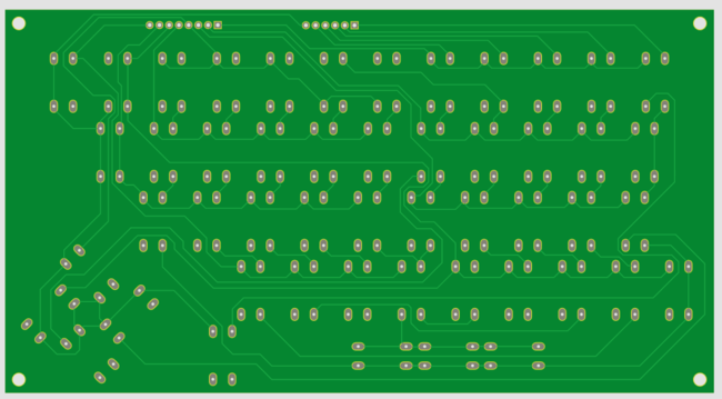
I have decided to use MCDTS-2 12 x 12mm keys with KTSC-21 (square white) key-tops for the keyboard. As all MCDTS-2 keys are sold in sets of 15, I have decided to use 45 keys, (5 more than the 40 keys an original spectrum uses). Inclusive the key-tops the price for the keys will be around € 17 (exclusive of the PCB they will be mounted on). The keys will have 12 x 12mm square tops with a flat surface, that can easily be labeled. They will be spaced out on a somewhat larger grid, with 3 or 4 mm room between the key-tops. The cursor keys will probably be arranged in a diamond shape (with keys rotated 45 degrees). Finished the keyboard schematic, added it to the .pdf schematics, above.
rendered a picture of how it would look, with keycaps removed:
About the expansion port pinout
Initially I choose to more or less copy the pinout of the ZX81 expansion port, but I do realize that there is no need to follow an existing layout. I should choose a layout that is easy to wire up. I realized that my ZX81+34 design has its expansion port not in the back, but more like a Sinclair QL on the left, and not on an edge connector, but on a dual row angled pin-header, which is a very good solution for mechanical and electrical stability. I also realized that I will more or less copy the same setup as the ZX81+34 design, with the expansion port on the extreme left next to the Z80 top left, the SRAM to the right of it, then the propeller to the right of the SRAM.
Power, VGA, and audio out connectors go on top, and the SD-card slot, and the DB-09 Joystick connector goes on the right hand side. Possibly I will add a simple power switch top right hand side too, meaning the power connector will move to the right hand side. it makes sense to do it like that.
That means that the most logical pinout for the expansion port would be to simply copy the pinout of the Z80. With the connections to it (between Z80, and expansion port), all routed horizontally on the same (top) side of the PCB, so that the other (bottom) side can be used for vertical connections (mainly GND and VCC).
So with the next iteration I will change the expansion port pinout to exactly follow the Z80 pinout. Obviously I will add extra signals like 3V3, SRAM disable, bank select and I2C signals as well.
As the pin-header is self aligning, there will be no need for the kind of "key slot" that an edge connector would use.
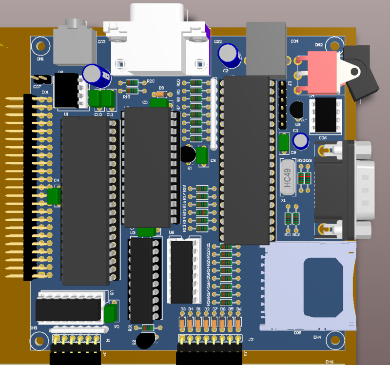
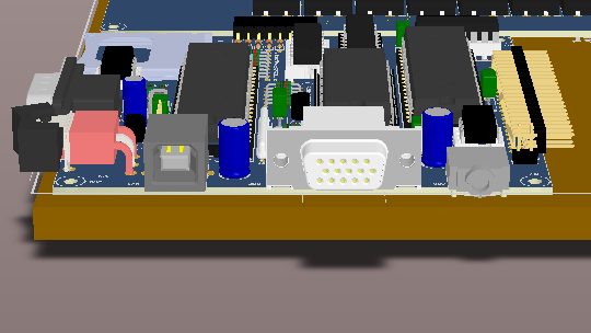
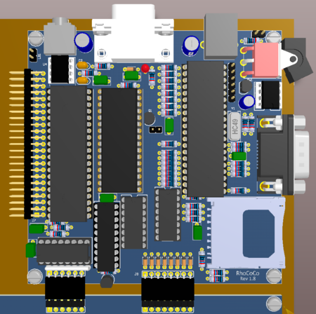
Created a (3D) preview of Rhococo
I was curious if Rhococo would fit on the same minimal 10 x 10 cm PCB that I managed to fit my ZX81 clone on. So I decided to quickly design a 3D preview to check, the preliminary conclusion is that I think it will fit! The first version lacked the various resistors, and caps, and the 3V3 regulator, but my guesstimate was that it would fit. On July 24, 2018, I added (almost) all remaining components on this preview, and as you can see they fit (which doesn't mean the PCB can be routed, we will have to see about that).
Here are a few preview pictures, seen from the top, and from the back:
Created a new set of schematic diagrams
This new set of three sheets replaces the older separate sheets, and has the latest corrections, for example a new expansion header, (replacement for the old edge connector) closely following the Z80 CPU, adding a power switch, replaced all hierarchical ports for the easier to use global ports, replaced resistors with SIP resistor networks, and a lot of other small corrections and changes, towards a version that is functionally complete, and has all the footpads needed. Consider this version 1.0. File:FULL RHOCOCO.pdf
Full schematics as pictures
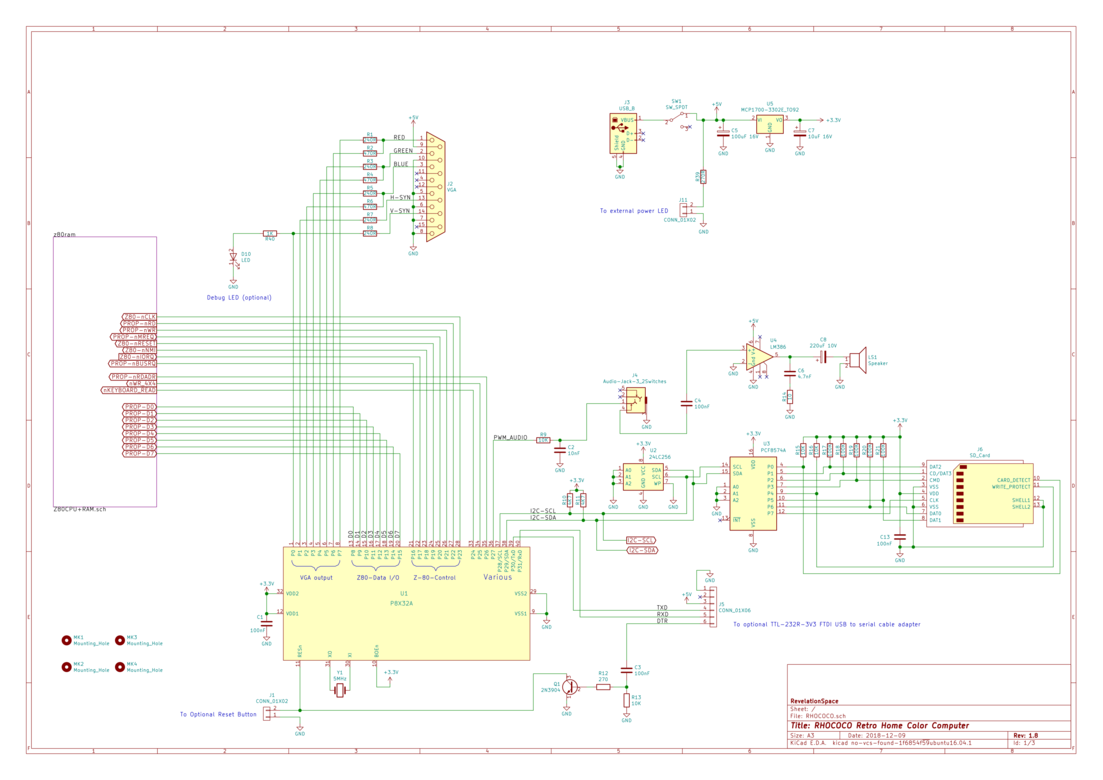
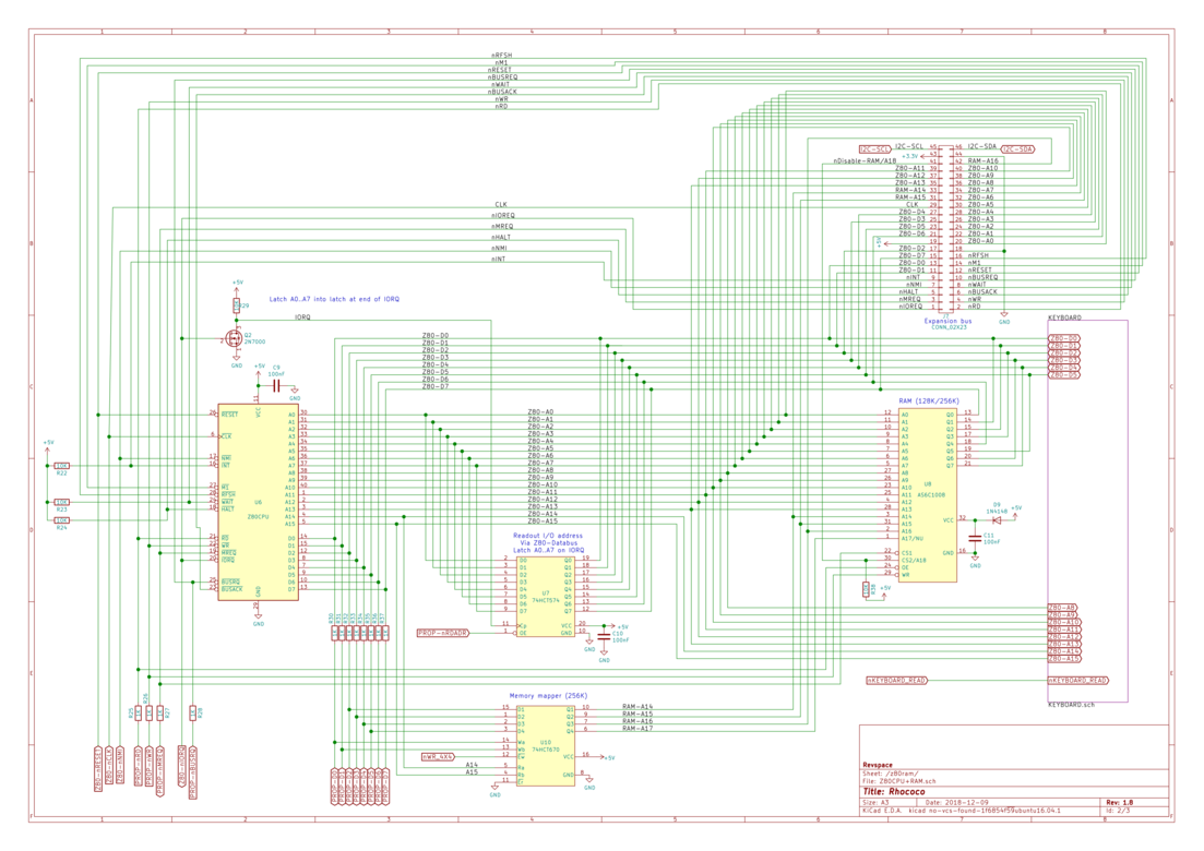
The pictures below are/will be always fully updated to the latest version (now rev 1,8 of December 9, 2018). Sheet 1 of 3: is the Main sheet. P1 to P7 of the propeller are used for the VGA output signals. So the propeller chip is capable of producing 64 colors per pixel, 8 times as many as a spectrum. Audio output is supported, as well as an SD-card (through the use of an I2C I/O expander).
If you want to see older versions, click on the picture an you will go to a page with intermediate versions.
Sheet 2 of 3: The Z80 (running at 5V) with its 128K/256K (eight or 16 banks of 16) RAM, and a latch that can capture the lower 8-address-lines during an I/O (write or read) operation, during the I/O operation the propeller can read out the data, and then the 8 address lines for an I/O write, or can read out the addresses, then put 8-bit data on the Z80 data bus for an I/O read operation. To the top right is the Rhococo specific expansion port.
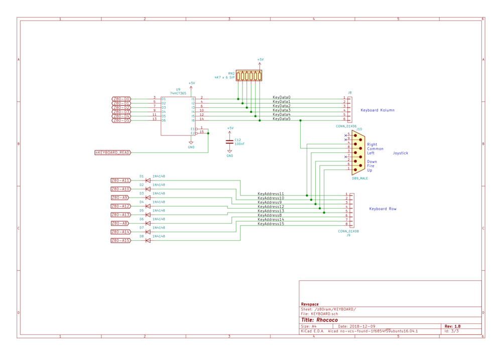
Sheet 3 of 3: Rhococo's keyboard is read by the Z80, and imitates a spectrum style interface, but the IO handler is driven by the propeller. The interface also supports cursor keys and a joystick port.
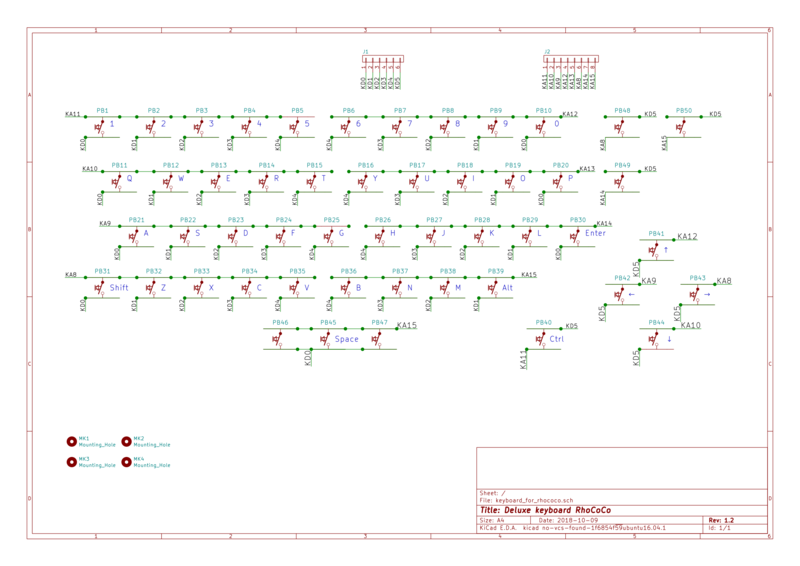
The keyboard itself is on a larger single sided PCB, connected with angled headers to the main PCB. this is the latest version of the schematic, the "deluxe" version for rev 1,8.
July 27, 2018 Changed physical width of RAM chip
I had chosen a slimline (300mil) P-DIP for the 128K SRAM chip, but I found out you cannot buy this chip in slimline form anymore, they are all 600mil (same width package as the Z80 and the Propeller). So I changed my Altium 3D renderings, luckily it doesn't seem to be a problem to accommodate the larger SRAM chip. Note that I can swap around address and data pins of the SRAM chip to ease routing. I moved the joystick connector down, as it conflicted with the switch. I will update all 3D previews.
July 31, 2018, finished schematics, and footprints, started placement of PCB
Made some minor modifications to the schematic, rotated the expansion header 180 degrees, as for the correct placement pin 1 should be at the bottom, not the top. Also changed the schematic symbol of the audio connector, to one that represents the SPC21348 better. Created footprints for the SPC21348, the VGA and DB-09 connectors, and started importing the components into the Layout editor. Drew a 10cm x 10cm PCB, and started placing the components within it.
This is the new .PDF: File:Full RHOCOCO rev 1.0.pdf
I also updated the schematic pictures above.
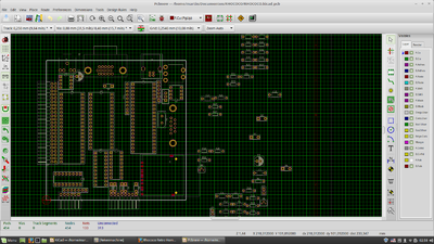
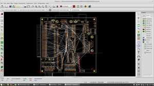
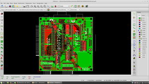
a screenshot of KiCad's layout editor during placement of the various components on a 10 x 10cm board, the ratsnest is temporarily turned off.
August 1, 2018 corrected some errors in the schematics and finished component placement
Found a few errors in the schematics, the z80 data-bus was reversed (D0 exchanged with D7 etc) a few times, and the order of wires to resistor pack RN2 wasn't optimal. Also added decoupling cap to J6 (the sd-cardholder). New schematic is revision 1.1: File:RHOCOCO PROP rev1.1.pdf
updated above schematics again.
I also finished component placement, as can be seen in this screenshot:
so now we have a valid ratsnest (the spiderweb of white lines) showing all the connections we have to create using the two copper layers of our dual sided PCB. As you can see its a bit of a daunting task. I think the first order of business is to try if we can simplify the job somehow by swapping address lines and data lines to the SRAM chip, because it really doesn't matter if any of the datalines (or address lines) is connected to a specific data (or address line), so we can swap lines to simplify routing. This means that the schematics could change because of this.
August 2, 2018 started layouting
I started by connecting the Z80 to the expansion port, and discovered the left and right column of pins should be switched, so I modified (mirrored the connector in the schematics, pin 1 is now on the bottom left, not bottom right. After that I routed data and address buses to the SRAM, to minimize trace lengths, I swapped several data lines and address lines to the SRAM, including the seventeenth address line (the bank select line). In the schematic it now looks a lot less straightforward, but I could connect all lines using only the top layer. the new schematic (so far) is revision 1.2; File:RHOCOCO-PROP Rev1.2.pdf
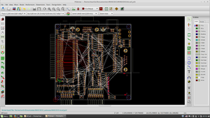
This is how far the layout has proceeded:
August 4, 2018 continued with layout
The main page of the schematic has changed, as connections between SD-card holder, and I/O expander chip have swapped to make the layout possible. the new schematic is revision 1.3; File:RHOCOCO PROP rev1.3.pdf the above picture is updated. This is how far we are now:
August 22, 2018 continued with layout, almost finished now
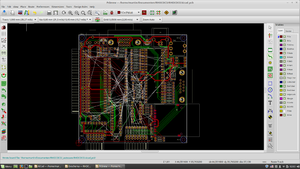
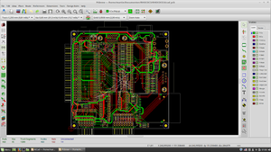
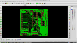
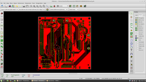
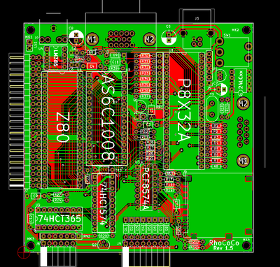
To be consistent with older layouts (mainly my ZX81+34 ZX81 clone) I changed (swapped) the colors of the layers, with the top side layer in green, and the bottom layer in red. You can see that green is the top layers, as its the layer the only SMT part, (the sc-card holder) is soldered on, the SMT pads are dark green. I made good progress, as can be seen in this screenshot, only 14 more traces, but the center is getting very crowded, its often the last 10% of the layout that takes 80% of the time:
August 29, finished layout, and copper fills
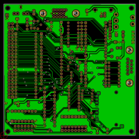
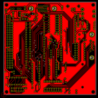
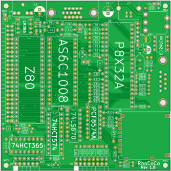
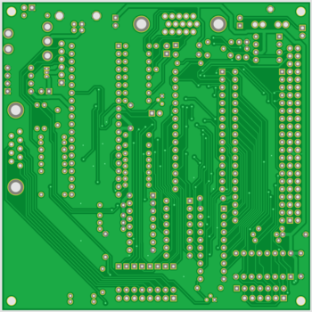
I completed the layout, the next picture shows an overview of the finished PCB, followed by the top and bottom copper layers.
next I will create the necessary production files, needed to order some PCB's, and I will design the single sided keyboard PCB.
September 3, 2018 Checked keyboard wiring, found and corrected some errors
Looking at the keyboard schematic, [2] I noticed the address lines are not in a logical order, while the keyboard connector address lines are, I have to correct that, and should also double check for other errors. My ZX81 clone keyboard worked fine, so I can use that as a starting point. After careful checking I concluded that the numbering and connector orientation of the keyboard schematic is correct, so from left to right the order of the connector pins is: KD0, KD1, KD2, KD3, KD4, (KD5) ---- KA11, KA10, KA12, KA9, KA13, KA8, KA14, and KA15, I have triple checked it with data from a real ZX81 to be sure.
So KD5 it seems, if used should be the to the right of KD4 The proof of the KD ordering is that KD0 is the most left connection, and goes to the 1/Q/A/Z row So both connectors have their pin 1 on the left side.
I should also switch diode references, so that D1 to D8 are used for the keyboard and D9 for RAM, so as to use the same references for the keyboard diodes as the spectrum, so D1 for A11, D2 For A10, D3 for A12, D4 for A9, D5 for A13, D6 for A8, D7 for A14, and D8 for A15. D9 will be used for the RAM power drop.
I will need to make corrections in the schematic and layout, luckily the PCB's were not yet ordered. It seems such wiring is always one of the things most difficult to get right, had problems with the same thing for my ZX81 clone, that's why I (luckily) decided to check it again.
I suspect the original KiCad footpads for the angled connectors must be modified, as with the 90 degrees bent forwards the pinorder is now reversed, with pin-1 being on the right hand side.
Actually what I think I will do, inspired by the Sinclair Spectrum, is to put the female headers on the main PCB, and the male headers on the keyboard. At least for the current angled 7 and 9-pin Pinheaders in the library, when rotated 180 degrees their pin 1's are on the left, as they should be.
September 5, 2018 corrected keyboard and sd-card
This was a big job, not only changing the keyboard interface wasn´t easy but I also had to create a footprint for the Molex 67600-8002 sd-connector, instead of the version in the KiCad library which did not conform to the sd memory card connector that you can really buy. The keyboard connector is now female, and has correct rotation, with pin 1 on the left side. address and data ordering is now correct (hopefully) The schematic has also been updated, and is now revision 1.4. This is the updated schematic File:RhoCoCo rev1,4.pdf.
And here are the pictures of the new layout:
checked the layout with a sample I got of the 67600-8002, (designing such a complex foot-pad is difficult, so its always a good idea to check it before using it in a PCB) and found that the pad on the bottom right should be moved a small bit to the right, and I should add two solder pads on the right side of the connector, for mechanical stability.
September 11, 2018 Corrected sd-card footpad
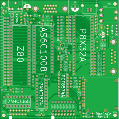
This is the new overview (rev 1.5) with corrected SD-card footpad, note the holes for plastic pins are gone, as no plastic pins were found on the sample cardholder I bought:
I have also started on the keyboard with KiCad. Designing schematic symbols and finding correct footpads for the switches and connectors in KiCads library, drawing the schematic of the keyboard, and importing the components of it into a PCB. I'm about halfway with that, after which I assume the single sided layout will be light work, next week I should be able to finish it.
September 14, 2018 PCB manufacturer preview RhoCoCo rev 1.5
I sent in the production files to a PCB manufacturer to check if it is manufacturable, which it was. No errors or problems. The result of the precheck is also in the form of a rendering of how the PCB will look like: Here is the top side, with silk screening and everything.
And here is the bottom side of the PCB.
This means I can start ordering the PCB's.
September 19, 2018 keyboard PCB layed out
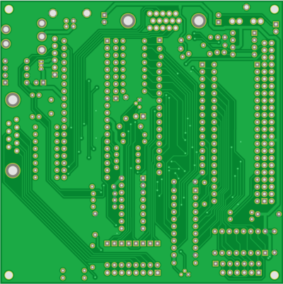
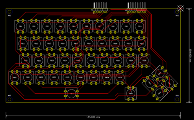
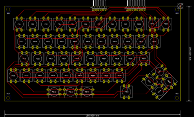
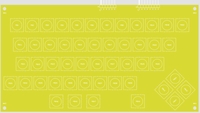
Designed a single sided PCB for the keyboard, using the fact that the used keys connect two pairs of their four pins. The following picture shows the layout for the solder side tracks, they layout could use some cleanup, but it has 100% connectivity, and no errors:
September 25, 2018 keyboard layout repaired, and optimized
found and repaired an error, optimized the layout for shorter traces, plus added drill holes. This is the new optimized layout:
I also generated gerber and drill files for PCB production.
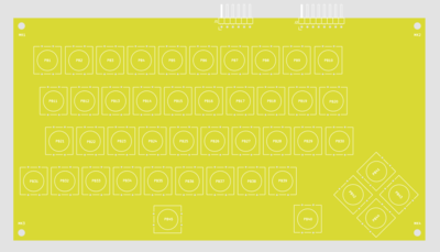
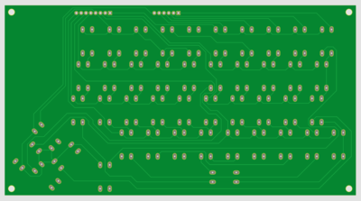
This is a picture (rendering) of the top of the keyboard PCB:
and this is the bottom:
I will now order the two PCB's from a PCB manufacturer.
October 3, 2018 PCB's not yet ordered, but started with propeller software development
Installed the propeller IDE (linux version) on my RevSpace laptop, and a dozen or so useful propeller objects to experiment with, including two types of VGA drivers, audio generator emulators, I2C, and SD-card drivers and much more.
I also took my propeller based "HYDRA Game Development Kit" [3] , (which I have had for over ten years) out of storage at home, and took it to RevSpace, so I could use it with the new (linux based) IDE, so I can start testing software on it. I also took extensive documentation about the Hydra, and the propeller from home to Revspace. The one thing I still need is a 9V DC supply with a barreljack, as the one that was in the Hydra box was an US 110V 60Hz version, I have several suitable ones at home still of this type ==>, which should be usable, after I make its adjustable voltage and polarity setting permanent with duct tape.
I'm waiting a bit before I'm ordering PCB's, as I have to do that from home, and I first want to refresh my experience with a propeller based system, so I can be sure that everything I do with the propeller chip on RhoCoCo works like I imagine it should. Explicitly I want to check if the USB-Serial interface logic I use is correct.
October 3, 2018 added some keys to "deluxe" keyboard
As I said previously I went for a keyboard with 3 x 15 = 45 keys, (because keytops are sold in sets of 15) however in the keyboard matrix there is room for 6 x 8 = 48 keys. When assigning characters I noticed that 45 keys is a bit restrictive, and it would be nicer to have a few more keys. Additionally the single key of the space-bar wasn't really a solution I was satisfied with.
So I added 5 more keys in this "deluxe" rev 1.2 version. Its still possible to leave the 5 keys out, for a cheaper version, but I think I will use the three added keys for special keys like backspace and '+' and '=' and such. Exactly what I will assign them for is still to be determined, but the preview pic on top gives an indication.
Note that if you leave the keys out you do NOT have to replace them with wire bridges. I have also moved the Ctrl key a bit to the left, in case you use it as the fire button in a game (as it corresponds to the trigger in a joystick, so is the keys that will be used as such in games)
here is the new schematic, File:Keyboard for rhococo rev 1.2.pdf and updated layout:
I also tried the Hydra, with a VGA demo, I could successfully upload the demo but it did not work. To be investigated, I'm not sure the Hydra still works, perhaps I need to replace the propeller chip. I noticed all supply voltages were a bit too low with 5V at 4.75V and 3.3V at 3.1V, not sure what causes it. Have to measure with an oscilloscope.
October 16, 2018 Finally got some life into my Hydra
The problems I had were mainly because the old power supply I tried to use it with did not generated a smooth DC, but a DC that consisted mainly of a large ripple. Probably the elco(s) inside it have dried out. After replacing it with a suitable supply I finally got a modified "blink LED" test program to work. I also tried to run several VGA generating programs, but none of them worked, probably because they were not written for the Hydra, but for another Propeller based board, or they were only "VGA drivers" without any main program that started (to use) them. This however did remind me that having a (few) "debug LEDs" on my board, and a power LED, would be a very good idea. So I will add some LED's to the RhoCoCo board, glad I did not order PCB's yet, this is one reason why its good to wait a bit before ordering PCB's. Without a debug LED bringing up a system can be hard.
October 23, 2018 added power and debug LED's
Added a series resistor and pin-header for the connection of an optional power LED, (to be mounted on the enclosure), and an on-board debug LED, (D10) which is connected to the pin used to select the second 64K RAM bank. This pin should be normally low, and as long as no Z80 code is running can be raised high, (to turn the LED on) without ill effect. Later when writing bank switching code the debug LED can also be useful. Here is the layout picture:
Note the power led connection J11, and series resistor R39 in the top right corner. The power on LED can be mounted on the enclosure, if you have one, or directly soldered to the PCB (to J11). The (optional) on-board 3mm debug LED is located somewhat below the VGA connector, and below it I managed to cram in its series resistor R40.
The one page that has changed for rev 1,6 of the schematic can be found here: File:RHOCOCO rev 1,6.pdf.
October 31, 2018, created production files of rev 1.6, and got VGA video out of my Hydra
I have tested the gerber files again, with Eurocircuit, for errors, there were none, I will start ordering some PCB's of both the Rhococo rev 1.6 PCB and its keyboard. I think I have waited long enough. Here is the rendering of the resulting PCB.
I also finally found a suitable VGA text demo that worked on my Hydra, and it should also work on the propeller chip of rhococo. The hydra uses a 10MHz crystal, not a 5MHz one like most other propeller system, and also has the VGA pins on an unusual range of pins, that makes that you need specially adapted versions of popular VGA drivers. I will use a 5MHz crystal for Rhococo (at least initially), and hopefully my choice for the VGA pin-group will not be a problem. In theory it should be easy to adapt VGA drivers for it, but we will have to wait and see how easy it will turn out in practice.
The current VGA driver (VGA.SPIN) I have now working generates 32 characters per line and 15 lines of text in 16 colors, which isn't ideal, and it uses quite a large font (the font built into the propeller chip), I want at least the same text size as a spectrum, (40 x 16 with my own font, or rather a graphical canvas in which I can draw such text). but for first proof of concept tests this 32 x 15 text mode will do.
Updated the concept artwork picture to rev 1.6.
November 6, 2018 found C64 like video modes driver
Found two screen drivers that emulate C64 screen modes, a two-color driver with the following specs:
Supported screen resolutions:
     320x240 Pixels, 40x30 Chars, 4:3 Ratio,  9600 Byte Buffer.
     160x120 Pixels, 20x15 Chars, 4:3 Ratio,  2400 Byte Buffer.
     384x240 Pixels, 48x30 Chars, 8:5 Ratio, 11520 Byte Buffer.
     192x120 Pixels, 24x15 Chars, 8:5 Ratio,  2880 Byte Buffer.
and an 4-color driver with these specs:
Supported screen resolutions:
     320x240 Pixels, 40x30 Chars, 4:3 Ratio, 19200 Byte Buffer.
     160x120 Pixels, 20x15 Chars, 4:3 Ratio,  4800 Byte Buffer.
     384x240 Pixels, 48x30 Chars, 8:5 Ratio, 23040 Byte Buffer.
     192x120 Pixels, 24x15 Chars, 8:5 Ratio,  5760 Byte Buffer.
Comes with the C64 8x8 character set.
I also found a variety of other VGA drivers, I can study to get some inspiration from.
The C64 drivers do not seem to support sprites, it might be possible to add these.
I noticed that almost all VGA demo's use a 5MHz Crystal, so I bought a 5.000 MHz crystal, so I can interchange it with the 10MHz crystal in my hydra (which luckily is socketed). It seems 5 MHz with a 16 multiply (for 80 MHz internally) is almost an universal standard, although there are people who drive a propeller with 100MHz.
November 13, 2018 I got a great idea, replace the Z80 with a -second- Propeller chip !!!
Luckily I still have not sent in the gerber files to create a PCB, as I suddenly had a brainwave. I was reading the site of "the 8-bit guy" which is a proficient you-tube vlogger specialized in retro computers, but he also has a web-site. I was reading there about his "ideal new home-computer", a subject near to my heart obviously. However his first requisite was that it should be 6502 based, and use "commodore BASIC" (read level 2 Microsoft basic with a screen editor). Now don't get me wrong, I like the idea of a screen editor, but the BASIC of a C64 was one of its biggest let-downs, it was exactly the same BASIC as the original Commodore PET, so very primitive. Still the request for a 6502 CPU wasn't so alien to me, I learned 6502 Assembler (on a MOS KIM-1) before I learned Z80 assembler, and I truly think its a great little CPU, and there are probably more home computers based on it than on the Z80. Unfortunately its very difficult to get your hands on a real one, and that will become only more difficult the next decades or so, so out of necessity I chose the Z80 instead. And yes, I do know the WDC 65816/65802 is still being made, but its not readily available to me, and could become even more difficult to get in the near future. Then I remembered that there is code for the propeller to emulate both a Z80, and also a 6502, so why not use a propeller running a complete chip-level CPU emulator for the CPU of RhoCoCo. You can choose the CPU architecture you want, either Z80 OR 6502, or for that matter you could emulate an 6809 CPU too if you wanted, or an 1802 or any other 8-bit (or 16-bit) CPU.
The 40-pin propeller has four 8-bit ports, so you can emulate an 8-bit databus, plus a 16-bit (or 17-bit for 128K) address bus, which leaves 7 or 8-bits left for "generic CPU signals". 2 bits to interface the emulated CPU to RAM with /OE and /RD, another 2-bits to directly communicate serially with with the other propeller, leaving 3-bits for IRQ and other signaling (IRQ and /IORQ for DMA between the two propellers, and one "/EXIO" signal for the expansion port).
sounds do-able, and offers much larger flexibility, such as direct 128K memory mapping with an emulated memory manager. with the real Z80 it should be possible to address 128K RAM, but only with a slow and convoluted method.
Because the CPU is emulated, you can do all kinds of special tricks that makes interfacing with the second propeller much easier, for example you need no special hardware to "catch" I/O addresses. And level conversion between 5V and 3V3 levels is not necessary, as both chips run on 3V3.
you only need one crystal, as you can clock the second propeller with the first, and both propellers can share the same reset. They cannot share the same EEPROM, but adding a second EEPROM should be possible. Especially as I can remove the 74HCT574 quad latch chip, needed to catch the IO request address. Which is not needed because we can catch it in emulation (and the 6502 doesn't even support IO mapped I/O). So there should be plenty of space on the PCB, after this simplification of the hardware.
You can upload code to the EEPROM of the primary propeller, then exchange the EEPROM with the EEPROM of the secondary propeller. So no special effort is needed to assist in programming the second EEPROM (although it should be possible with a few jumpers to switch between using the serial interface for inter-propeller communication, and programming either one of them).
So that is what I am going to do the coming weeks, I will redesign the current implementation to one that uses two propellers. Obviously I will first backup my original design.
I'm not going to give this version a new name, I will still call it simply RhoCoCo (not RhoCoCo 2 or RhoCoCo ][ or something like it). Because the first version was never finished anyway.
I almost have the feeling that this idea was the last piece of the puzzle, that I felt was still missing, (perhaps unconsciously the reason I hesitated to call the design finished) and now I found it.
whether RhoCoCo will become a Z80 based or 6502 based system has now become a moot point, it can be both, but as I found both a 320 x 200 40-columns C64 graphics driver AND a SID chip driver, and the new found memory mapper capabilities maybe a "C64" clone (or rather work-alike) computer could be a good choice, but with the BBC BASIC of the real 6502 based BBC Master.
November 16, 2019 Well, unfortunately its seems the disadvantages of this approach outweigh the advantages, so Ill keep the Z80
After careful consideration, there seem to be too many disadvantages to an emulated CPU, and no real advantages. For example It seems there is no good P8X32A code to do full 6502 emulation. And using a propeller to emulate a Z80 means that the expansion port becomes almost useless (too many signals simply would disappear from the expansion port). And I hear that the emulated Z80 would be much slower than the real Z80. RhoCoCo would also look much less retro without a real Z80, and the whole project would become much less simple to understand. In other words its not KISS compliant.
I have been thinking about adding discrete components to support bank switching, but I would need at least a PAL/GAL like device to do it, and it wouldn't fit, so I would have to enlarge the board, and make the design much more complex. In the end I don't think its worth it. I can still code routines to copy data from/to the second 64K bank, without adding any extra hardware, this will give me much of the advantages of bank-switching without needing extra hardware.
November 20, 2018 Considering adding bank switch support with 74LS670 IC
On the raspberry PI forum, where I have a thread about RhoCoCo a member called "Hippy" hinted that I could solve the bank switching problem by using a 74LS670 4 x 4 bit register file. This is just a small 16-pin DIP IC, that contains all the logic that is needed. I have not yet tried to figure out completely how to integrate it in the rhococo, but it seems possible, so my first thought was, "can I fit it in", is there physical space for it left on the PCB, so I returned back to my Altium 3D preview mockup, to see if I theoretically could find room for it, and I did (which doesn't mean layouting it is possible). This is a preview of the 3D rendering of Rhococo with an added 74LS670 (U10) Revision 1.7.
I started stripping the current layout, and moved the VGA driver resistors to port1 (Pin 1 to 8), and am also trying to move the 74HCT574 as far as possible to the left, in an attempt to create space for the 74LS670. I removed the pull-down resistors of the data-port's 5V to 3V3 divider, as I learned that the propeller is 5V tolerant if you limit the current flowing into the GPIO port (with a series resistor) so the lower resistor of the divider isn needed. I have moved the data-bus for port 1 to port 3, (pin 21 to 28), but this might change to port 2 (pin 13 to 20), if that helps simplifying the layout. its a lot of work, and it might be that I'm trying the impossible, or it doesn't clean enough space to add the 74LS670.
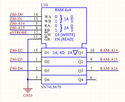
as for using a 74LS670, I studied the datasheet, and now understand how I can use it. its essentially a programmable address line re-mapper, that remaps A14 and A15 to A14' A15' and A16'. so that any combination of A15/A16 can result in any (programmable) combination of A14/A15 and A16. The result when used for a memory mapper is that the memory is divided in four sections of 16K, and that you can put any of the eight 16K blocks of the 128K RAM at any of the four 16K blocks in memory. To remember which block appears where in the memory map, the chip contains four 3-bit words, 4 bits of the register array are not used. the mapping can be programmed with six data-bits, and a strobe, the strobe being the re-purposed A16 select propeller GPIO bit.
This is how I think the 74LS670 should be wired:
Note that Z80-A14 and Z80-A15 are used to select one of the four bits that contain the settings for RAM-A14 RAM-A15 and RAM-A16. The bits are programmed using Z80-D0 .. Z80-D5, two databits are used to select one of the four bits, and three what the bits should contain. To program them the Z80 is halted, and tri-stated, so that the propeller can drive the data-bus, (ViH of the 74LS670 is 2.0V, so logic level compatible with the 3V3 levels of the propeller). This programming can be done before the Z80 is started, so that the bits can be set so that the four 16K blocks appear in their logical order, from the first 64K bank of the RAM. After this is done the propeller can then initialize the RAM with BOOT and BASIC code. In a more conventional system the lack of a reset input on the 74LS670 would have been a major problem, for in the addition of extra hardware to circumvent the 74LS670 before code could boot.
I have moved the debug LED from this mapper strobe GPIO bit to V-Sync of the VGA output, as putting it on the re-purposed GPIO bit is no longer a good idea, and V-Sync is a better solution, also the debug LED is probably no longer needed when VGA is working.
I think the layout work will take at least a few Tuesday evenings, and Saturdays, hopefully I can make it fit.
P.S. the LS version might have a problem with the series resistors in the databus, the best solution would be to use the data signals directly from the propeller. or use a HCT version instead, but these are hard to get (in DIP form).
November 28, 2018 Started with new rev 1,7 schematic, and layout, with 74LS670 memory mapper
Cleaned up schematic, and added 74LS670 memory mapper, initially for 128K RAM (eight 16K pages) later (if I succeed with the layout) I will try to fit traces for 256K support. here is the new schematic (rev 1,7):
I think I did 80% of the layout work.
The white lines are connections I have yet to do. As you can see I temporarily removed the copper fills. Updated the 3D picture above, and the impression picture, and tweaked the placement of parts in an attempt to fit all the connections in, especially made more room between the 74LS670, and the IO-Expander chip, as I expect to need to fit more traces there. As I'm gaining more confidence it will fit I have updated the main 3D impression picture on the top of this page too.
December 2 Various layout jobs
Updated the schematic to rev 1.8, with support for large ROM's on the expansion port. And done more remaining layout work (as shown in the updated picture above). I updated the keyboard layout too, as I moved the left keyboard pin-header connector a tiny bit, and so the keyboard had to be corrected too, and I have put "74LS670" on the silk screen. I have also routed the RAM-A14, RAM-A15 and RAM-A16 lines to the expansion port, instead of the Z-80 A14 and A15, so that an (up-to) 128 K RAM/ROM on the expansion port can disable (part off) the RAM and take its address space, or possibly expand it.
December 5, 2018 Finished 100% routing
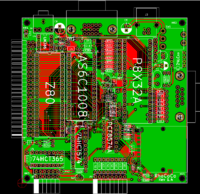
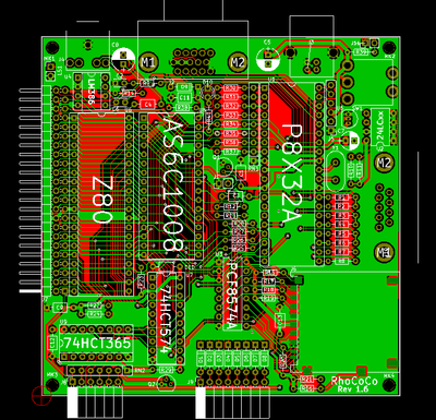
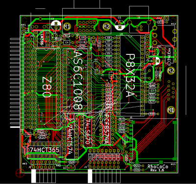
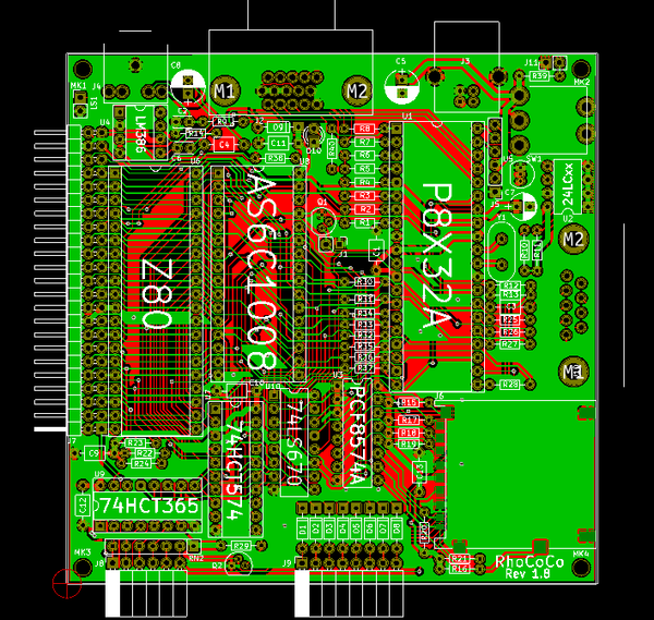
PCB is fully routed, so I did it! Amazingly it fits, although at the end stage I started worrying if it could, without switching to a higher density layout (with 0.15mm wires instead of 0.25mm, so I could route two lines between two pins with a pitch of 1/10". That would have made the PCB less easy to produce, so probably much more expensive. This result still needs some cleanup work, and optimizations (especially of the ground plane copper fill) but I now know that it is layout technical possible to integrate the 74LS670! Here is the picture of the 100% laid out board, still revision 1,7 (will update to revision 1.8 after cleanup, optimization and final checks).
I realized that if I manage to route a wire from pin-1 of the RAM chip to the unused output pin of the 74LS670, and add another data-line from the propeller data port to the 74LS670, it would be possible to use the memory mapper to address 256K of RAM (not eight, but sixteen 16K pages). It would be a missed chance if I did not try to add this option too, even if I will not initially use 256K RAM's (they are harder to find, as the 512K versions are more common). an initial observation of the current layout does not immediately disqualify the possibility that adding these connections is possible. P.S. After looking at the layout I wondered why pin 3 of the LS670 wasn't connected to GND, so I looked at the schematic, and realized that the data-line is already routed to the propeller, so all I need to do is to add the wire to pin-1 of the RAM chip.
December 9, 2018. Finished rev1,8 with 256K memory mapper
The new schematic is here: File:RHOCOCO rev 1,8 schematic.pdf
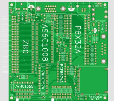
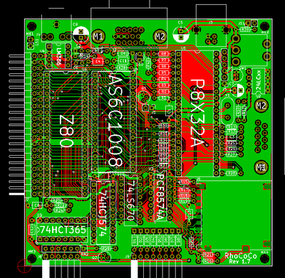
The picture of the finalized, Design rule checked, and optimized (especially the groundplane/copperfill) is this:
I made gerber/drill production files, and will test upload them ASAP. If all is well, I will order some PCB's for the main dual-sided 10x10cm PCB, and the keyboard PCB.
I have updated the schematic pictures of "Full schematics as pictures" halfway this page.
I will describe the ordering process in another project page.
December 10, 2018 final checked PCB layouts
Layouts are okay, the PCB's will look like this:
and finally the full 3D rendered preview of rev 1.8:
And yes, its really very compact, the "main PCB" measures just 10 x 10 cm, and so the whole thing is just a little bigger than a ZX81, about the size of a Matra Alice, or Tandy MC-10, but which much better specs.
December 10, 2018 made preview of the Rhococo in an enclosure
Just for fun, and so you can see how big it will be, I rendered a picture of Rhococo in a half transparent red plastic enclosure, (in the style of the French Matra Alice home-computer [4] ). For size comparison I added a match. This picture I used for the "designing an enclosure for RhoCoCo" wiki page. [5]
December 18, 2018 modified keyboard PCB
I have done some last minute tweaks on the keyboard PCB. I removed 8mm square areas from the front PCB corners so that the keyboard can be mounted inside of an enclosure with screw positions in the corners of the enclosure. The cutouts make space for plastic structures for the screws.
I have also enlarged the pads for the 6-wire and 8-wire connectors. I now plan to solder flexible cables to the keyboard, and expect somewhat larger mechanical forces on the connector pads of J1 and J2, so I gave these solder-pads a bit more "flesh" so the adhesion of the copper pads to the PCB has become a lot stronger.
January 29, 2019 Ordering the PCB's
I ordered the PCB's with the Chinese PCB manufacturer PCBWay. I made a separate project page about it.
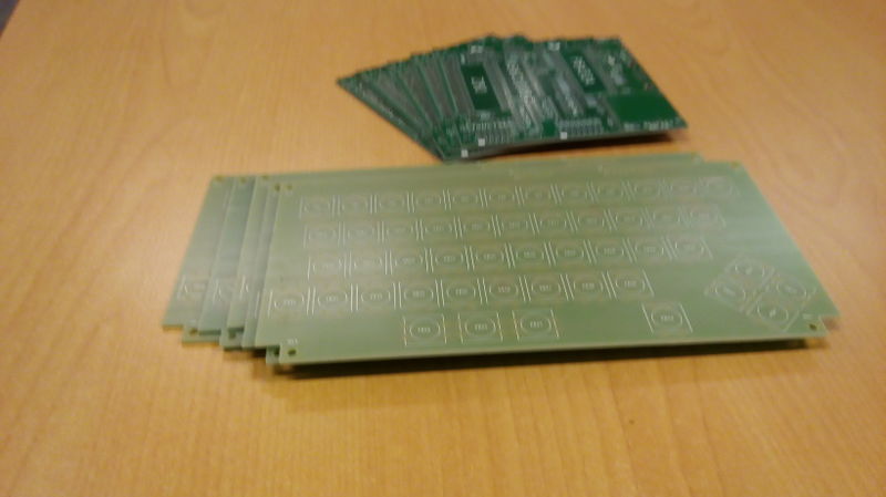
March 7, 2019 PCB's are in
They look good. Next step creating a complete Bill of materials.
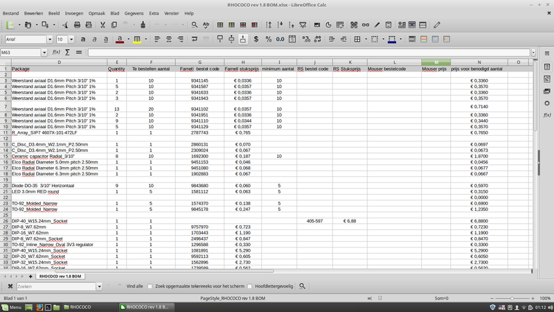
March 20, 2019 Finished Bill of materials
The price for parts, for the first prototype (without PCB's, or enclosure) comes to around €71, for main-PCB, and €32 for the keyboard. So around €103 for a single prototype board (without PCB's)
The integrated circuits alone are not the most expensive, around €20, and the connectors alone cost €33.
Obviously The price can go down substantially when you order multiple sets of parts, and for the cheaper parts the minimum order quantity is often larger than you need for one prototype.
Ordering parts for a second and third set would not have a great influence on the price, as often you need to buy at least five of something for the price to go down, so initially I will only order parts for one prototype. Ordering a second and third (or more) sets later won't mean I loose much money.
A .PDF version of the BOM can be found here: File:RHOCOCO rev 1.8 BOM.pdf
March 27, 2019 Ordered all components
The stuff that came from a special vendor (RS and Mouser) were ordered for all 5 prototypes, and I ordered three 20MHz Z80's and two 10MHz ones to experiment how fast I could clock the Z80. The rest was ordered from Farnell, simple to order stuff in unity, some for 3 or 5 boards. Expect to have it all before the end of the week.
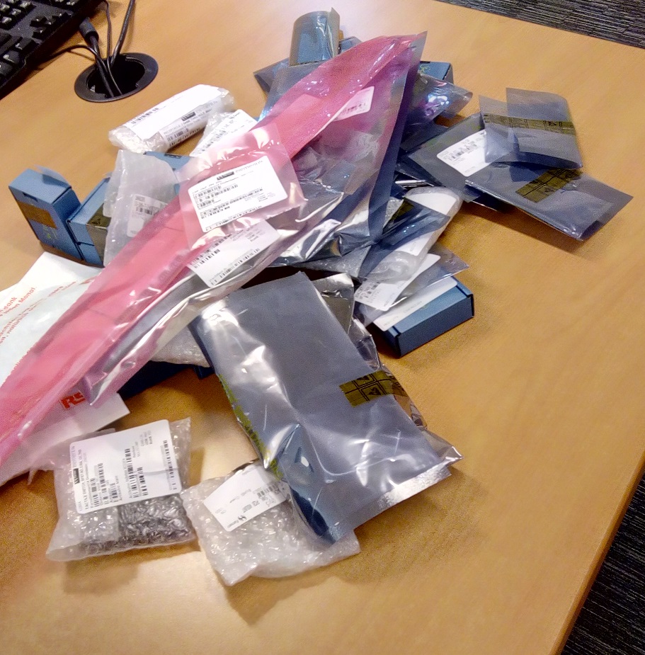
March 28, 2019 Parts are in!
Parts I ordered from Farnell, and RS are in, Mouser parts come later today or tomorrow.
This weekend, during the open day of Revspace, I will start building up the first prototype.
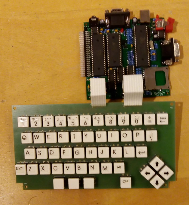
April 3, 2019 Prototype is finished
Here is a picture of it, freshly assembled:
This ends "designing the RhoCoCo Retro Home COlor COmputer hardware" page, at least for this hardware revision (rev 1.8).
Now I have to do some basic measurements, to see if all is well with the hardware, see https://revspace.nl/Rhococo_prototype_hardware_debugging, and after (hopefully) fixing any issues that I find, I can start to think about developing software, where I will probably (possibly) find new "hardware challenges".
First tests, and experiences done during building up revision 1,8 lead to revision 1,9.
April 24, 2016 Redesigned PCB rev 2.0
This is the corrected schematic, File:RHOCOCO rev2.0.pdf
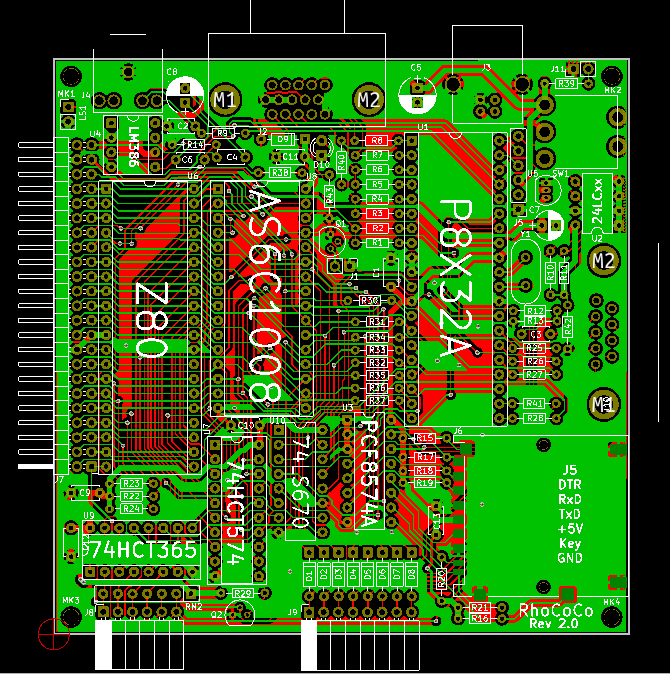
the new layout looks like this:
Note that all capacitors now have the same 5mm pitch, R41 now limits the current from the z80-IORQ signal, added the new load resistors R42 and R43, the resistors R30 to R37 now have more room, and I put text on the PCB, visible through the opening in the SD-card holder describing how to wire J5 for serial programming. Lastly I added holes for the plastic alignment pins of the card holder.
I changed the resistance of the current limit resistors in the Z80 control outputs to the propeller from 1K to 15K, as they are active from the start, and active low, so normally high. The data-lines are inactive until the propeller starts the Z80 (and produces a clock signal) so their resistance doesn't have to be increased and so I kept them at 1K, also because they also go to the address mapper 74LS670 that need LS level input signals to be programmed. I will start developing firmware with the 74LS670 replaced with simple wire links, so that the 74LS670 cannot be a problem during firmware development, only after the Z80 runs code reliably, I will add the memory mapper.
I also patched an extra 15K current limit resistor for IORQn which I forgot to add.
I found that I had disabled the internal pullup resistor on the RESETn line by tying the BOEn "brownout control" line high, I repaired that in revision 2.0. For the prototype I added an external pullup, as patching the PCB was too cumbersome.
I found an USB-Serial dongle which will work to connect my laptop to the Propeller of the rhococo, I already installed the Propeller IDE on my laptop, and tested it with my Hydra. I will create a fairly long 5-wire serial interface cable so I can put the USB dongle directly into my laptop. I used the dongle to upload a LEDblink program to the propeller chip, so the propeller is programmable, and programs can be saved in its EEPROM.
A new page about booting up RhoCoCo (about bringing up firmware and software development) can be found here: https://revspace.nl/Bringing_up_Rhococo_(first_boot,_and_firmware_development) where I will continue reporting about the progress of developing firmware, and getting Rhococo working.
Keyboard connections error discovered?
while creating a keyboard PCB for my ZX-81+35 I noticed there seems to be an error where I switched A12 and A9, I will investigate, and correct any errors in the main and keyboard PCB's. I do understand the problem could be fixed with software, but I do want to keep compatibility with a read ZX-81/Spectrum keyboard if at all possible, so I will resolve errors if I find them.
Keyboard connections are not wrong, only the spectrum, is not ZX-81, compatible
I discovered these is a difference in the order of address lines used between the Zx-81 and the Spectrum, in a spectrum, compared to a ZX-81 A9 and A12 have swapped, so the schematic is still okay.
I think I found a solution for the generation of an SPI signal for the SD-card reader
I was having trouble generating an SPI signal, with just a simple PCF8574A I2C I/O expander, the I/O expander I choose is very primitive and (although I remain unconvinced it cannot work) gave me too much problems in converting existing SPI bit-banging routines that directly worked with Propeller GPIO pins, to a solution that worked over I2C.
The solution I have devised is using an I2C to SPI bridge chip, the SC18IS602B. Its a very small TSSOP16 IC, I can put on a small carrier board that I can plug into the socket of the PCF8574A I/O expander socket.
During the Covid-19 lockdown I thought things over
And came to the conclusion that I'm probably approaching the SPI problem from the wrong angle. I will research the possibility to create a simpler solution that uses GPIO pins for SPI, even if I have to rethink other aspects of the way I'm using the propellers GPIO's. even if I have to make drastic layout changes.... well see.
Hopefully I will be able to drag myself out of Covid hibernation....
