ZX81PLUS35 ZX81 clone: Difference between revisions
m (→5 January 2016) |
|||
| Line 237: | Line 237: | ||
== 5 January 2016 == | == 5 January 2016 == | ||
Here is the latest preview, seen from the front of the board, the picture is fully updated, and also includes the planned ZX81+35's expansion board. | Here is the latest preview, seen from the front of the board, the picture is fully updated, and also includes the planned ZX81+35's expansion board. | ||
[[File:ZX81+35 revision 2.2 december 2015 front preview.png]] | [[File:ZX81+35 revision 2.2 december 2015 front preview.png|1000px]] | ||
The expansion board can also be used as an extender to give the edge connector some people want, either on the left, or by extending the top of the board, even on the back. | The expansion board can also be used as an extender to give the edge connector some people want, either on the left, or by extending the top of the board, even on the back. | ||
A planned enclosure (casing) will enclose both the main zx81+35 board, the keyboard and the optional expansion/extension board to guarantee a sturdy whole. | A planned enclosure (casing) will enclose both the main zx81+35 board, the keyboard and the optional expansion/extension board to guarantee a sturdy whole. | ||
== 10 January 2016 == | == 10 January 2016 == | ||
I have also made a new component overview drawing, which I can use when placing components on the board for reflow soldering: | I have also made a new component overview drawing, which I can use when placing components on the board for reflow soldering: | ||
Revision as of 22:29, 23 January 2016
The ZX81+35, previously called the ZX14, and ZX15, and ZX81+34 (2015 Version) retro homecomputer is a much improved Sinclair ZX81 [1] clone built with the modern materials techniques and components of 2015. The ZX81+35 will be built and tested in 2016.
it will be fully open sourced effort (but note that the original design of the ZX81 and its BASIC interpreter firmware is still owned by Amstrad)
As for now comments and questions on the design can be made here [2] (raspberry PI forum off topic section) :-)
Introduction to the ZX81+35
The ZX81+35 is a much improved ZX81 that people can build themselves.
The ZX81+35 should be fully compatible with the original ZX81, but with the following improvements over the original ZX81 :
- Includes turbo option switch giving more than double (220%) the speed of the original, with turbo LED, and dynamic turbo slide switch.
- Includes 16KB of RAM instead of the original 1K (should also support 32K mode) but should be compatible with "high resolution" software.
- RAM can be made permanent with a battery backup system (optional) so program remains even during power off
- Supports ZX81 BASIC in either a EEPROM or in an OTP (one time programmable ROM) P.S. version 2 uses FLASH with a total of 16 8K banks.
- Compatible with modern TV's thanks to better digital sync signal generation, giving sharp stable and high contrast pictures.
- Composite video (PAL or NTSC) output signal instead of RF signal, for even sharper picture, compatible with yellow RCA inputs, and SCART
- Wobble free real expansion connector (can be modified to be fully compatible with the ZX81) modules can fit inside ZX15 enclosure, compatible with ZX81 printer
- Uses simple microUSB chargers as power supply, with low power consumption
- Can drive a simple 2x16 LCD display, and some external I/O for "stand alone" applications like driving tiny robots. Debug LED/Backlight LED support.
- Simple sound generation (full sound only when using fast mode)
- Supports a DB-9 joystick with up-down-left-right and fire, immediately compatible with games that use keyboard arrow keys (5,6,7 and 8) and 0 for "fire"
- Supports keyboard with real (moving) keys, using new keyboard overlay with holes for the keys, uses cheap 6x6mm buttons, keyboard layout also available. Using the original keyboard is also possible
- More sensitive and reliable cassette tape interface (can be reliably driven by MP3 players and such)
- Includes reset button option, and power LED.
- Alternative (nicer) ZX81+34 font available, to replace the standard one in the ROM.
- No need for the original ULA, it is replicated with conventional logic.
- Cheap to build by using low cost components, on small dual sided PCB, with single sided assembly only.
- Design files will be freely available (but do note that firmware is still © Amstrad!)
Status, from January to march 2015
At the moment the PCB of the first prototype (ZX81+34) has been designed, and is ready to be tested.
26/01/2015 2 PCB's are being made, waiting for delivery next week, also a component order list has been created. 27/01/2015 A component placement diagram has been made, and has been published here. 31/03/2015 one PCB has been assembled, a keyboard is being made, (the first keys I bought were unsuitable due to too short plungers so I bought new ones. A programmed EEPROM needs to be made, I will probably design my own EEPROM programmer. Problem is that I used a 32K classical EEPROM, which has a different pinout than 64K and bigger sizes, for which FLASH versions are available. This means I must use a real EEPROM programmer, instead of being able to flash program the PROM. Ill design a raspberry PI based simple programmer, also useable for other replacement of other RETRO EEPROMS.
25/09/2015 could not get the first model to work (found faults in the schematic, but main problem is that many of the logic circuits were damaged when I applied the 5V with reversed polarity due to a wrong microUSB definition). Started on revision two, with all the bug fixes and acquired knowledge.
3D Preview of early ZX81+34
Before I even designed the PCB I made a mockup with Altium. Here are two (3D rendered) previews of the ZX81+34 board, to the top one is an older small preview of the complete system, including how I envisaged the whole system with keyboard would look like, at the bottom you can see a picture of the more recent 3D rendering of ZX81+34 PCB, and to the right, as a size reference the original ZX81. Note both PCB's are about equally as tall (10 cm), but the ZX81+34 is much smaller, as it square, while the ZX81 is much wider than it is tall.

The botom picture also shows, on the right, the four chips of the original ZX81, and on the left, what replaces them on the ZX81+34, green is the Z80 CPU, RED the (EE)PROM, Yellow the RAM (1K on the ZX81, 16/32K on the ZX81+34). Blue indicates the logic of the ULA, contained in a single 40-Pin IC on a ZX81, the ZX81+34 replicates it with 24 conventional but modern logic ICs.

Schematic 81+34
The old (version 1) schematic of revision 2.0 (.PDF) can be found here: File:ZX81+34 schema.pdf
There is also a color coded schematic (.PDF), it can be found here: File:ZX81+34 kleur REV 2.0.pdf.
Note that SMT components are depicted purple, and PTH ones green.
The Bill of Material (BOM) for the original ZX81+34 can be found here File:Z81+34 BOM.ods

Layout ZX81+34
Even though I was hospitalized, then immobilized for several months (in the months of June July and August 2014) due to an operation on my leg, I still managed to work a bit on the layout of the ZX14. And on November 25, 2014 The layout work reached 100% connectivity. Here is a preview of how the work was progressed at that time . Clean-up, optimizing and copper filling followed somewhat later. The picture below on the left was actually a screen shot from a gerber viewer of how the board looked in September 16, 2014, note the lack of copper fill to make it easier to follow the connections around. Some weeks later the cleanup was ready, and this is a picture of how the PCB will more or less look like, when it is finished.


Keyboard for ZX81+34/35
Early on I was also busy designing a solution for the keyboard. My solution was to use commercially available cheap 6x6mm buttons, which (with some effort by bending the pins a bit) can be mounted on an EuroCard sized piece of 1/10"raster perfboard, the result would like something like the picture on the left.
Here is the schematic (plus board layout) of the keyboard: File:KB matrix schematic.pdf
I also designed a new keyboard overlay suitable for such a keyboard with the keys going through holes in the overlay. On the right is a drawing showing how it would look, note the brown dots are actually the actuators of the push buttons going through the holes in the overlay.
Here is a .PDF version that should be correctly scaled when printed on A4 paper. You can also use it to create a replacement keyboard for your ZX81.
A version that supports the ZXPand can be downloaded here: File:New ZX81+34 keyboard ZXPand version.pdf


Alternative font for ZX81+34/35
I also designed an alternative (fun) font for the zx81+34 that can replace the one in ROM, it should be compatible with existing software, so graphic symbols are unchanged. As inverted characters are a hardware function, inverted characters (and graphics) are simply inverted copies of the original characters. Here is a preview.

Here is the original ZX81 character set to compare it with.
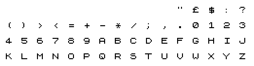

I know that big changes were not possible, but note for example the 4 and the A X and Y, and the addition of serifs to many characters.
The final ZX81+34
Finally mid January 2015 the PCB of the ZX81+34 was finished, a grounded mounting hole was added (needed to mount in an enclosure, to shielding). The picture below is a 3D rendered preview, some of the texts on the preview are there to comment some of the functions, and will not be present on the silkscreen of the final PCB.

The assembly drawing of the ZX81+34
Here is a drawing to help assembling the right components at the right places (A placement drawing), it was made from the real silkscreen gerber-file (in red) comments and component values in black.
Note that the values of R39 to R40 are wrong, they should be 22K not 1K!

Starting the assembly

just started with soldering the various resistors with a hot air soldering station
Finished assembly

Assembly of the ZX81+34 and its keyboard has finished. Still waiting for a programmed EEPROM before it can be tested.
The bare board looks like this:

Design of a (wooden) enclosure has started, also there is a chance I can lend an EEPROM programmer.
Testing (continued)
After I finally managed to program an EEPROM, I started testing the device, unfortunately disaster struck immediately! I could not get the device powered up, and after some searching I found out I made a mistake in the creation of the footprint of the microUSB connector, that caused the reversal of the GND and 5V pins. This means that for some time (minutes) the whole device was fed with negative 5V, a disaster! From previous experience I know that most CMOS devices can survive this, with the exception of (older types) of EEPROM's which are often erased by feeding the wrong polarity of signals. The EEPROM used 28HC256 is more modern, so I have some hope it has survived, time will tell. P.S. I have since verified that the EEPROM indeed was not affected! Normally I add protection in the form of a 1N4001 diode between +5V and GND, but because voltage inversions normally cannot happen with an USB fed design I failed to take that precaution. :-(.
A very bad start indeed, its possible/likely that any and all CMOS logic was destroyed.
After fixing the polarity problem, (with a nasty patch consisting of first using the microUSB connector upside-down, later replacing it with a short cable to a type B USB port) I tried powering on again, and 5V came up with just 100mA consumption, but no life in the system. I found the main (13MHz) crystal oscillator was not running, and the problem seemed that the footprint for the crystal was for a 5 x 7mm device, while the only 13MHz crystal I could find was a 5 x 3mm device. The crystal seemed not to make contact. I replaced it for one that could be soldered to the edges of the crystal, but the oscillator still did not ran! I tried replacing the 33pF load capacitors with 15pF ones, but no luck. The "tiny logic" inverter used in the oscillator seemed to work with static logic signals, but did not want to oscillate, perhaps it was "blown up", I replaced it, and after some effort the oscillator proved to be working (jay!). I followed the clock signal through the timing chain, and it seemed to be working in all the SO-logic devices, but when it came to the last buffer before clocking the Z80 that tiny logic buffer U25 failed! It was in a difficult place to desolder, and I had no replacement, so I arranged for a new one, to be de-soldered at work, where I can re-work with hot air under a microscope. Meanwhile the microUSB connector had fallen off the board (sigh, ripped off is a better description), and was replaced by a contraption with a normal size USB type B connector on a small PCB, its ugly but it works.
After looking at the Z80 clock driver I realized I used open collector driver, without a pullup, after adding a pullup I had my z80 clock, but the system was still dead, I have since reverted the driver to a inverting push-pull (type HC04) driver. I realized what pain the current location of this IC is, very hard to re-solder.
With the Z80 not running, I tried to debug the Z80 logic, and found that the very first instruction the EEPROM does after reset is an OUT,&FD instruction, but that OUT,&FD was not happening! Perhaps the Z80 was blown up. I found a bug, namely the reversal of VCC and output pins of U17 (single gate OR), I fixed that with a patch, but the OUT&FD was still not happening. I replaced the Z80 with an old 4MHz Z80 I had, but with no luck (no video). Careful examination of the schematics revealed a few other errors, explaining the lack of video. The SH/LD signal must be driven by pin 8, not pin 9 of U29B, The CSYNC signal should be an XOR of VSYNC and the inverted HSYNC, not HSYNC itself, so pin 1 of U21a must be tied to pin 11 not pin 13 of U21C, also the clock inputs of U28 were not driven by the /WR signal, as they should have. So I added the corrections to the schematic, now convinced I needed to create a new PCB, I also switched the OTP in the schematic to the EEPROM I used.
I posted the new revision 2.0 schematic here, and patched the board. Later I found that the pullups on the databus were 1K, I forgot to change them when I copy pasted them, leaving them at 1K cannot work, as the databus series resistance between memory and CPU is also 1K, so the restores act as a 1K,1K voltage divider, and only halve the voltage arrives! Changed the pullup resistors to 22K, that should work.
I still had to test if the patches I found, and the new Z80, have solved the problem, If not, I have to resort to using a logic analyser to find the problem, that would be a bummer! But no luck, my ZX81 clone still did not work. I finally gave up and tried a (simple 8-channel) logic analyzer, and quickly found that half the databus signals were permanently low.
some databits, but not all, seemed to be driven low permanently by U1, the NOP driver. after removing U1 the databus seemed okay, but replacing U1 with a new one did not solve the defect. arrrgh.... That was the moment I decided not to search for more defects, probably lots of logic ports are blown up! But instead to take my losses, and immediatley create revision two of the ZX81+34 (even when it meant it would become a ZX81+35 in 2016) .
So without further ado, I present to you the first changes for ZX81+34 rev 2.1 AKA "version two".
ZX81+34 version TWO
The main schematic difference, (except the removal of some faults) with this second version, is that I switched the EEPROM over to FLASH, with pulldown resistors for unused address lines, perhaps I can connect these to a rotary 16-position selector switch to switch between various ROM images, later.
Here is the new schematic revision 2.1:
 A .PDF of the new schematic can be found here:
File:ZX81+34 rev 2.1.pdf
A .PDF of the new schematic can be found here:
File:ZX81+34 rev 2.1.pdf
Note that many changes I will make to the new board will not be expressed in the schematic, but rather in the layout, some planned changes are larger pads for the 0805 devices, other footpads for the diodes, now in 0805 shape, relocation of some components, changing the footpad of the crystal, changing the DB-9 connector to an normal angled version, so it does not fall below the bottom of the PCB, relocation of the elco, and changing the microUSB connector to a better type, (while fixing the polarity bug) and perhaps other small fixes and tweaks and corrections I might yet find. My aim is to create a ZX81 clone that works, is as "timeless" as possible, (meaning it's components will still be available in another 30 years time) and is easy to build.
3D preview version 2
I planned which changes I'd have to make, and how that would influence the 3D preview, and changed it accordingly, the most eye catching change will probably be the DB9 connector which now is connected through a short six wire cable, instead of being soldered to the edge of the PCB, but there are may other changes. One visible change in this rendering is that the Z80 is now placed in its socket. But there are other small changes too.

Version 2.1
October 6th 2015; found another error, labels of OUT_FE and OUT_FD were interchanged, which influenced the turbo logic. Also replaced the DB9 connector with a 6-PIN Pinheader. The DB9 is no longer soldered to the board, but connected with a 6-wire flatcable connected to the right DB9 connector pins. Uploaded new schematic version 2.1, which replaces Rev 2.0. October 21, 2015, updated schematic, .PDF of schematic, and PNG 3D view. Removed buffer, added extra elco changed µUSB connector to FCI type, like in 3D view.
Version 2.2 (ZX81+35)
November 24, 2015; Just when I wanted to order new PCB`s when I received a Tip from some ZX81 hardware experts that there was an "error" in my schematic. I`m resetting (synchronising) the free running cycle counter with the VSYNC signal, which according to them is wrong! Instead I should use the interrupt acknowledge signal, which is the AND of /M1 and /IORQ. Although almost all the previous ZX81 clone circuits which I have seen use the VSYNC signal (like the ZX97, most of rodney Knaaps rebuids and the ZX81 ULA Replacement By Andrew Rea) I`m fine with that and understand why it is better, and am willing to just add a single NOR port for it, a single extra SOT23-5 tiny logic device should fit. But before I do this I will discuss it with these ZX81 experts on their forum at http://www.sinclairzxworld.com/viewtopic.php?f=7&t=1780#p18255 as soon as I have registered there.
The delay now will guarantee that my ZX81 clone will NOT be released in 2015, so I`m (yet again) changing the name, too (surprise surprise) "ZX81+35" In the hope it will finally be finished in 2016. Remember I started with it in February 2014!
In the mean time I managed to get Circuit Maker (The free Altium-like CAD package) working on my ancient Lenovo T60 laptop (thanks go to my RevSpace mates) so my next projects will be done with Circuit-Maker instead of the ancient Ulticap/Ultiboard software I used up-to now.
The first project with CM will be a re-build of the Magnavox Odyssey, the very first video game system see also https://revspace.nl/Magnavox_Odyssey_Rebuild.
Discussion with the forum members of sinclairzxworld.com is ongoing, and it seems there could be an error in my 207 step line counter logic, (affecting hsync and back porch generation) which will be resolved before ordering new PCB's.
December 9, 2015 Mayor changes Revision 2.2
To make a long story short I indeed accepted that the line counter should be synced with intack, not kept pending for the duration of VSYNC like my earlier version, that also meant I had to re-think the logic for HSYNC and porch generation. While doing that I discovered my earlier porch logic was faulty (used the low nibble, instead of the high nibble of the counter), anyway the new logic should generate a sixteen cycle HSYNC signal sixteen cycles after the intack, and the back porch lasts 16 cycles after that. Here is a .PDF of the latest schematic, revision 2.2; File:ZX81+35 REV 2.2.pdf
Here is the latest drawing, with a better resolution than previous attempts, thanks to an online .PDF to .PNG converter.

I have changed the XOR U31 into a AND, with /VSYNC and /HSYNC (active low inputs) as that seems to give a better CSYNC signal, this means That I will change the connection to PIN 2 of U31 from VSYNC to /VSYNC. I was also attended to the fact that U30 isn't a latch as I wanted, but instead was just a buffer! Darn! I replaced it with a real latch, a 74HC574. Added R54. Hopefully that will be the last design error.... I have started with the layout of this version. Some strategic planning indicated that I can place the four SOT23-5 devices, as in this 3-D view, three to the bottom left of the Z80 (above the random logic) and another one to the right of the random logic.
A user of the ZX81 forum expressed the desire to have the DB9 directly soldered to the board, or with a 2x5 pin flatcable. I decided that an angled DB9 connector could be used if either the connector did not have a shell, or it had a plastic shell, like farnell #1075281) but would be mounted on top of the few SMT connectors, the latter situation I have expressed in the 3D rendering preview above. It is also possible to use a super cheap (less than an Euro) "Stamped Pins" DB9 connector, and wire it to the board with (short stiff or long flexible) wires.
29 DECEMBER 2015
Finalized the revision 2.2 layout, just before year end.
This is how the new revision 2.2 layout looks, note that unlike the previous version I left out copper fills.

An attentive visitor to the ZX81 forum made me aware that the label for the I/O expansion latch port was incorrect, as /OUT_FE, it should have been /OUT_7F, the corrected schematics (Picture and .JPG) have been updated.
30 December 2015
I noticed I could replace one IC (U10, a 74HC1G04) with the unused inverter of U21, I did that and renamed U31 to U10, and also added one more decoupler cap, and I updated the changes in the layout, and did some final optimizing of power traces, and rearranged silk screen texts to horizontal.
I updated the layout picture, and the schematics, as seen above.
5 January 2016
Here is the latest preview, seen from the front of the board, the picture is fully updated, and also includes the planned ZX81+35's expansion board.

The expansion board can also be used as an extender to give the edge connector some people want, either on the left, or by extending the top of the board, even on the back.
A planned enclosure (casing) will enclose both the main zx81+35 board, the keyboard and the optional expansion/extension board to guarantee a sturdy whole.
10 January 2016
I have also made a new component overview drawing, which I can use when placing components on the board for reflow soldering:

23 January 2016
On the sixth birthday of Revspace I finished the BILL OF MATERIALS for the ZX81+35, here are its two pages as pictures:
