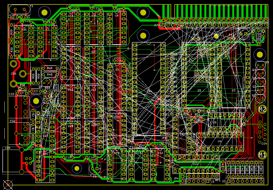
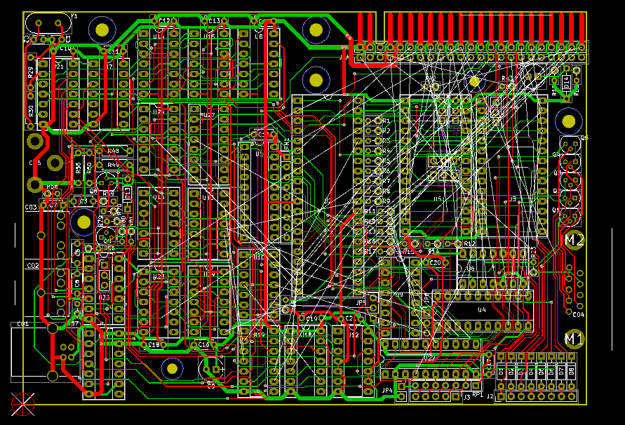
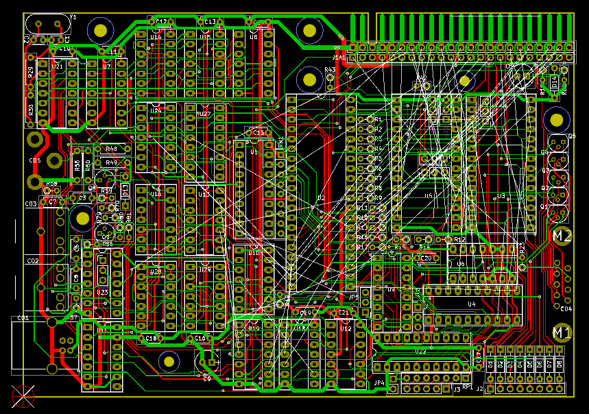
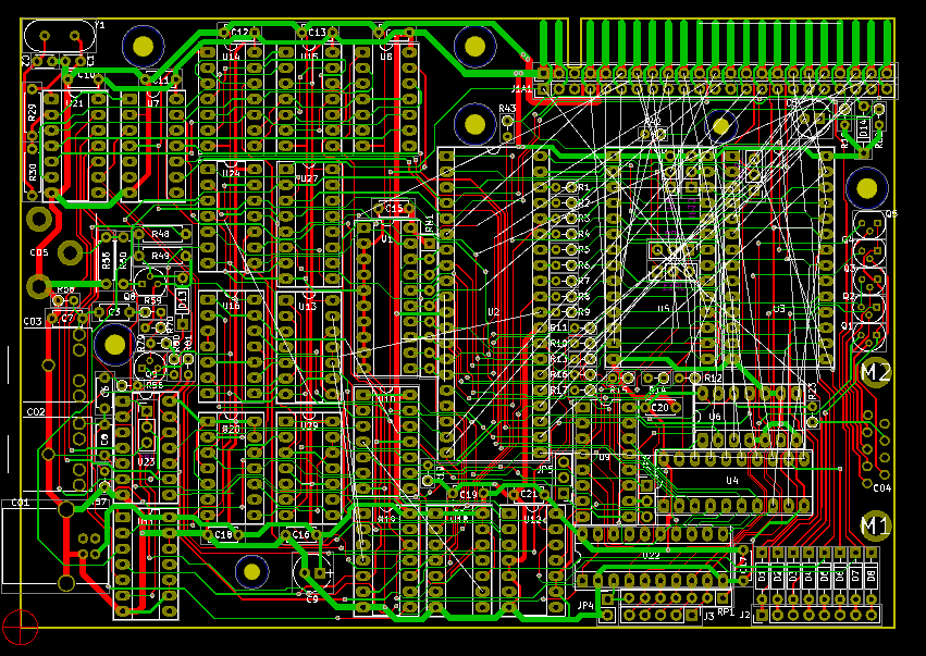
ZX81plus38 simple to build ZX-81 clone: Difference between revisions
No edit summary |
|||
| (363 intermediate revisions by the same user not shown) | |||
| Line 1: | Line 1: | ||
{{Project | {{Project | ||
|Name=ZX81plus38 | |Name=ZX81plus38 | ||
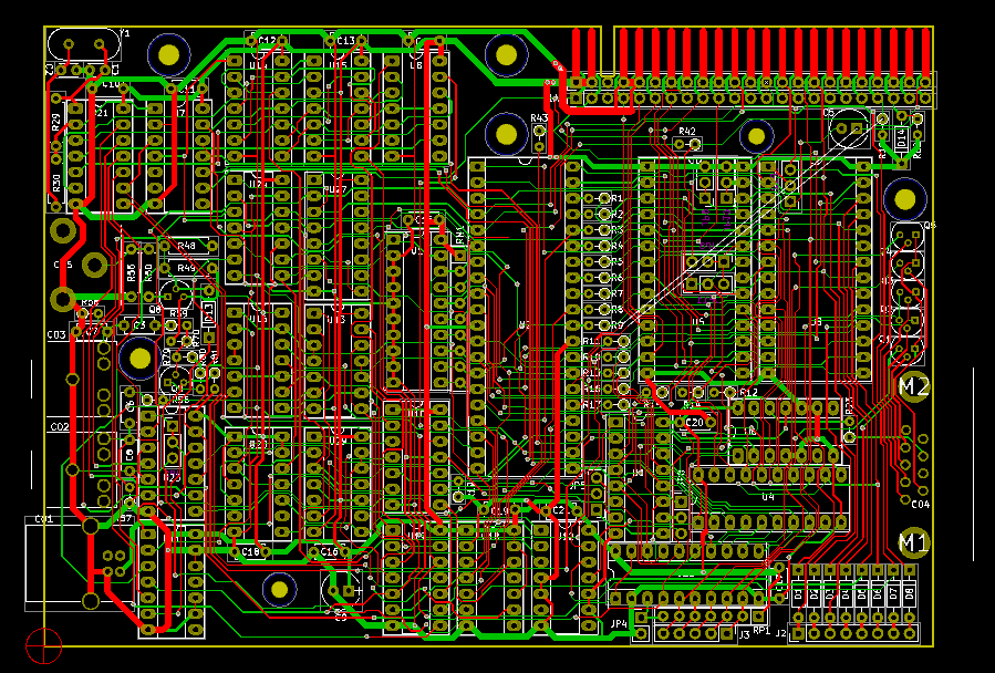
|Picture= | |Picture=PCB Preview ZX81+38 rev 1,10 top now with PSG expansion board.JPG|px500 | ||
|Omschrijving=Most people I showed my ZX-81 clone (ZX81+35) said they liked it, but with such a tiny board and with so many "difficult" surface mount components, | |Omschrijving=Most people I showed my ZX-81 clone (ZX81+35) said they liked it, but with such a tiny board and with so many "difficult" surface mount components, they doubted whether they would be able to build this kit, so I restarted my effort, to try to build a 100% compatible ZX-81 clone that anybody could build, but now with commonly available pin-through-hole parts. | ||
|Status= | |Status=In progress | ||
|Contact=mahjongg | |Contact=mahjongg | ||
}} | }} | ||
| Line 11: | Line 11: | ||
For now I will call it ZX81+38, but I doubt it will be finished in 2019, so it will probably be renamed to ZX81plus39... :-) | For now I will call it ZX81+38, but I doubt it will be finished in 2019, so it will probably be renamed to ZX81plus39... :-) | ||
P.S. No I won't! | |||
I started analyzing my current schematic, to see whether it contains components that are not available in PTH, and unfortunately there are some, for example "unbuffered inverters" (74HCU04) used in the crystal oscillator, are no longer available in DIP. Also some other logic isn't available in DIP, 13MHz crystals are hard to get in PTH versions, and 6.5MHz are not available at all. | I started analyzing my current schematic, to see whether it contains components that are not available in PTH, and unfortunately there are some, for example "unbuffered inverters" (74HCU04) used in the crystal oscillator, are no longer available in DIP. Also some other logic isn't available in DIP, 13MHz crystals are hard to get in PTH versions, and 6.5MHz are not available at all. | ||
| Line 25: | Line 27: | ||
== September 24, 2019 I placed most of the components in the schematic == | == September 24, 2019 I placed most of the components in the schematic == | ||
I was curious if my USB replacement logic would fit, so I quickly placed most of the needed logic in the schematic, and annotated them the same as my SMT version (logic simplification and renumbering will come later), and gave them PTH footprints. At the end of the evening I had enough of the schematic elements to do a forward annotate, so I could do an estimate of it would fit, the result is visible in the top right hand corner of this page. To my relief I found that it should fit (its just a rough estimate obviously). | I was curious if my USB replacement logic would fit, so I quickly placed most of the needed logic in the schematic, and annotated them the same as my SMT version (logic simplification and renumbering will come later), and gave them PTH footprints. At the end of the evening I had enough of the schematic elements to do a forward annotate, so I could do an estimate of it would fit, the result is visible in the top right hand corner of this page. To my relief I found that it should fit (its just a rough estimate obviously). | ||
== September 29, 2019 continued with component selection and routing of the schematic == | |||
I found out which combination of gates and such resulted in the fewest physical IC's, swapping some gates around, and trying to find replacements for single gate IC's, which do not exist in DIL. changed the AND that combined HSYNC and VSYNC to and EXOR as during VSYNC HSYNC pulses actually appear as inverted in the VSYNC signal, but perhaps I should check my logic here carefully. | |||
I also changed the AND combining video with the nPORCH into a NOR, with inverted inputs, also something to check later. | |||
I had forgotten how much trouble it is to get the connections of the Z80 databus to the NOP enforcer, and pullup resistor pack right, probably I will need lost more wire swapping action to get a somewhat easy to route solution.Laying out this board will be an interactive and iterative process, with lots of forward annotations, and corrections in how everything is connected. I won´t swap data and address lines around for the EPROM (or we have to do some swapping of the EPROM content too, and that is not what I want). This implies that RAM lines swapping won´t happen either, as the ROM and RAM wiring is almost identical. | |||
== October 1, 2019 continued == | |||
Stupidly I lost previously placed mounting holes, that took hard work to do , because I imported a schematic that didn't have them, so the forward annotate function removed them from the board. I noticed they were gone when I looked at the preview picture. | |||
So after uttering a few choice words I have now entered mounting holes in the schematic, and once again started with their placement. Luckily I had made a 1:1 (real size) printout of the PCB WITH the locations of the mounting holes, which makes measuring up their locations a tiny bit easier. Now I also differentiated between 3.0mm holes for the screws that close up the case, and slightly smaller (2.5mm) holes for mounting the PCB to the enclosure. | |||
I also re-read some old correspondence about using an EXOR for combining HSync and Vsync, and saw that there are technical reasons why using an simple OR function will be better, So I will do that instead. I also realized that from revision 2.2 to the current revision 4.0 of my ZX81+35 the sync generation logic has had a big overhaul, that has never been tested. Also I was warned that my component placement drawing of ZX91+35 contains an error, listing U13, as a 74HC32, (OR gates) instead of a 74HC00 (NAND gates). I wanted to check if the BOM had the same error and tried to download it from GitHub, but for some reason I only got a .ZIP containing gibberish instead of the spreadsheet. Both problems I will fix soon. Also the person who noticed the U13 problem also has problems with horizontal sync not being present, and I have to investigate that too. | |||
He promised to send me one of his two build up prototypes that have this problem. | |||
on a positive note, he is using my keyboard PCB too, and it is working fine! | |||
== October 6, schematic mostly finished == | |||
Yesterday I finished placing of the mounting holes in the PCB, today I mostly finished the schematic. | |||
Replaced main picture with the preview schematic as a .PNG picture. | |||
== October 9, schematic rev1.0 finished == | |||
Schematic finished for rev 1.0, updated schematic [[File:ZX81plus38.pdf]], plus preview schematic pictures. | |||
Next up, importing the components in the PCB layout, and placement of the parts. No attempts have been made yet to try to support multiple types of ROM/EPROM/FLASH, like the original ZX81 ROM. | |||
But this schematic should be complete. New is my attempt to support the canonical cassette loading video bars. | |||
== October 13, 2019, schematic rev1.1 (some errors fixed, added ZX81 ROM support) == | |||
Found, and repaired some errors, when doing electrical rule checking, (non connected power supply pins, no footprints assigned, such errors). nNMI is now directly connected to A6, without a resistor in-between. Improved the way cassette input shows up as loading bars by using and AND port. Noticed many labels where the "'" (bis) marker was changed to something very similar, but resulting in no connections between various connections having a "'" (bis) sign in the label, checked all nodes with a bis marker (D0' to D7' and A0' to A8') for connectivity, and repaired the labels with a problem. Also, I corrected some labels where I used the backslash to denote in inverted signal, instead of the lowercase "n" I used everywhere else. | |||
also found a small error in the original ZX81 schematic, which claims that the D7 signal is NOT connected through a 470 Ohms resistor, but actually, it IS! (I measured 470 ohm between pin 13 of the Z80 and pin 1 of side A1 on a real ZX-81), so the "D7" label on the expansion connector should have been written as "D7'". | |||
Added several 3-pin jumpers so that the EEPROM socket can be configured to accept a ROM from a real ZX81, These jumpers are pre-connected, and per default configured for a 27C256 EEPROM, two of the jumpers can also be used to select one of four possible 8K images that can be contained in a 27C256, per default only the first 8K is used. Jumpers will be "virtual", meaning they will probably be mounted on the underside of the PCB under the EEPROM, and to change for a ZX81 ROM you will need to scratch through the pre-connection between pin 1 and 2. | |||
All components are now cleanly forward annotated, so next job will be component placement. | |||
Schematic is now revision 1.1 [[File:ZX81plus38 rev 1.1.pdf]] | |||
== October 15, 2019, finished schematic rev1.2 (functionally complete) == | |||
Added support for loading bars, using spare gates, only new part is one pull-down resistor. added some explanatory texts, changed U22 so that its wiring is optimal for keyboard column readout placement. converted the logic type to active low logic symbols where that was more logical, so its easier to follow the logic. | |||
This schematic should be functionally complete, (if nothing unexpected happens) changes beyond rev 1.2 should only consist of pin or component swapping optimizations, and component renumbering (after I did the placement). | |||
Revision 1.2: [[File:ZX81plus38 rev1.2.pdf]] | |||
== October 20, 2016 rev 1.3 supports 16K ROM's == | |||
I realized that some people might want to extend the Sinclair BASIC ROM, or replace it with something else, and might need a larger ROM, so I added a (virtual) jumper to enable 16K ROM's to the ROM encoder and added A13 to the EEPROM address lines. | |||
revision 1.3 with 16K ROM support: [[File:ZX81plus38 rev1.3.pdf]] | |||
== October 30, 2016 First component placement == | |||
I managed to place all the components on the available IC's,but barely so. | |||
[[File:ZX81+38 component overview proposal.png|px800]] | |||
I will probably need to do a lot of optimization (IC and gate swapping) to minimize as much as possible the routing needed, as there is almost no space left for routing. | |||
== November 6, 2016 re-shaped the DIP pads to accommodate routing two wires between pads == | |||
As you can see in this picture, on various places it becomes impossible to do horizontal routing of connections, if you can only route one trace between two pads. | |||
[[File:Ratsnest ZX81+38.png]] | |||
You can also see I modified the PADs to make this possible, I decided to use a PAD height of 60 mil (with a hole size of 35mil, and a pad width of 90mil), so there is 40 mil between two pads, for two traces you need two traces of at least 0.15mm inter-spaced with three spaces of also at least 0.15mm. | |||
So 40 divided by 5 = 8mil, or 0.2032mm. I decided to use 0.2mm traces . | |||
Next job is to simplify the rats nest by swapping ports (and or components). | |||
== November 13, 2019 Did a lot of placement optimization == | |||
Now the schematic is updated to revision 1.4. [[File:ZX81plus38rev 1.4.pdf]] due to swapped ports. | |||
Not only a lot of ports have been swapped, but also the component placement itself has been modified a lot. | |||
This is revision 1.4 as a 16 color .PNG (in full resolution), open to see full resolution. | |||
[[File:ZX81plus38rev 1.4 16 colour.png|1000px]] | |||
== November 20, 2019 finished placement, did some power routing == | |||
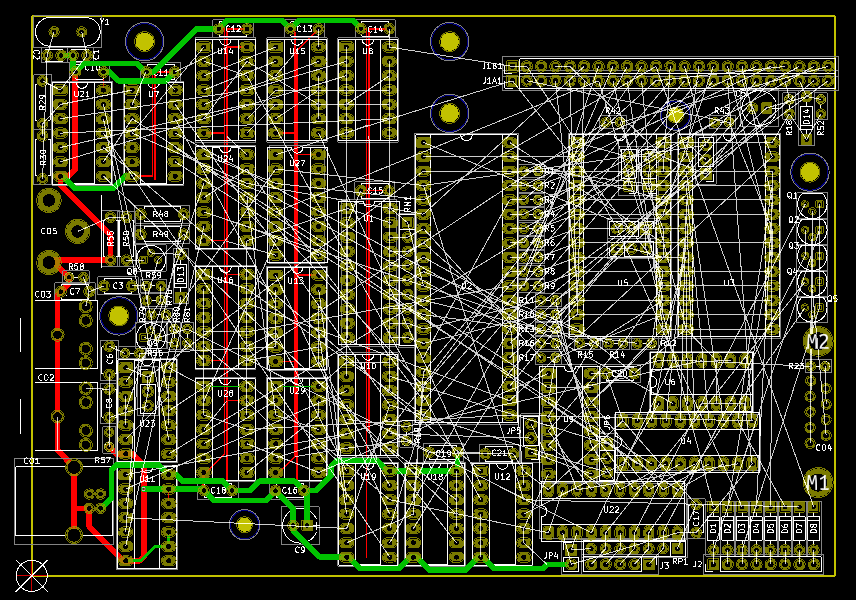
based on schematic rev 1.4, I further optimized placement and started with power routing (GND and +5V) as the basis. | |||
This screenshot shows my progress: | |||
[[File:Placement and ratnest 2019-11-20 02-05-42.png|1000px]] | |||
== December 10, 2019, partially routed == | |||
routing proceeds nicely, this is the current situation a few weeks later: | |||
[[File:ZX81plus38 routing progress 10 december 2019.png|1000px]] | |||
== January 14, 2020, some progress == | |||
The easy part is done, routing now becomes more difficult. | |||
[[File:Ratsnest ZX81 plus 38 14 jan 2020.png|1000px]] | |||
== January 22, 2020 more progress == | |||
[[File:Ratsnest ZX81plus38 22 jan 2020.png|1000px]] | |||
== January 28, 2020 == | |||
[[File:Ratsnest ZX81+38 28 jan 2020.png|1000px]] | |||
== February 12, 2020 == | |||
[[File:Ratsnest ZX81+38 12 Feb 2020.png|1000px]] | |||
Removed a lot of connections to the expansion connector, as to improve the overview of the connections. | |||
As for now, power and databus connections are present, as well as a few address lines. When the currently active connections are done, I will start adding address lines, and the most important control signals, then attempt to add the rest of the connections. | |||
== February 19, 2020 == | |||
[[File:Finished layout ZX81+38 19 feb 2020 without copper fill.png|1000px]] | |||
Finished routing! Also Added enough connections to the expansion port so that I/O based expansions boards should still work (printer, Programmable sound generator board, joysticks etc). Memory expansion is not really useful, nor DMA. so it is not supported. in practice this should not be a problem. | |||
After I finish extensive cleanup I will add copper fill (GND). | |||
== February 26, 2020 == | |||
I decided to do an ultimate attempt to route the missing signals to the expansion connector, so that I could also support external memory, and I succeeded in routing almost all connections, just two signals /BUSACK and /WAIT are not connected, but I'm planning to attempt these next week. :-) | |||
[[File:Ratsnest ZX81+38 26 Feb 2020.png |1000px]] | |||
== March 4, 2020 layout finished == | |||
Finished /BUSACK and /WAIT, did DRC checks, added copper fills. created gerber files to do a productivity check. | |||
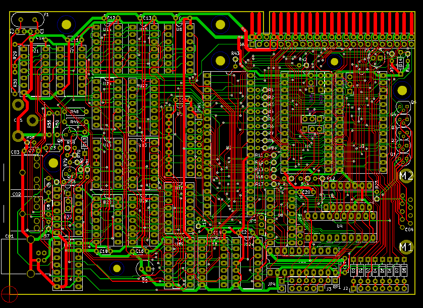
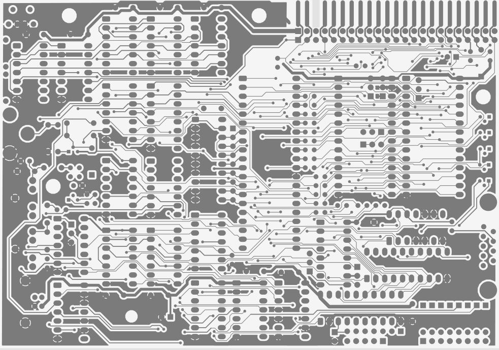
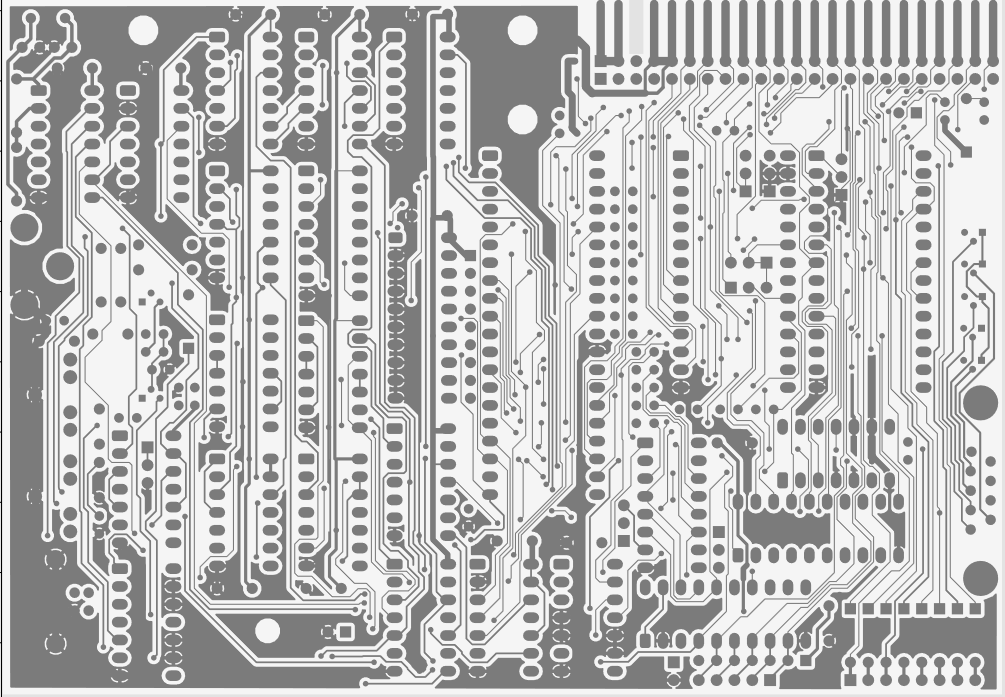
[[File:ZX81+38 4 maart 2020.png|1000px]] | |||
I uploaded the file to a PCB producer to check it for aberrations (violations of their production rules) and I'm happy to say there were none. | |||
This is how the top layer (without solder mask) would look like: | |||
[[File:ZX81plus38 copper top.PNG]] | |||
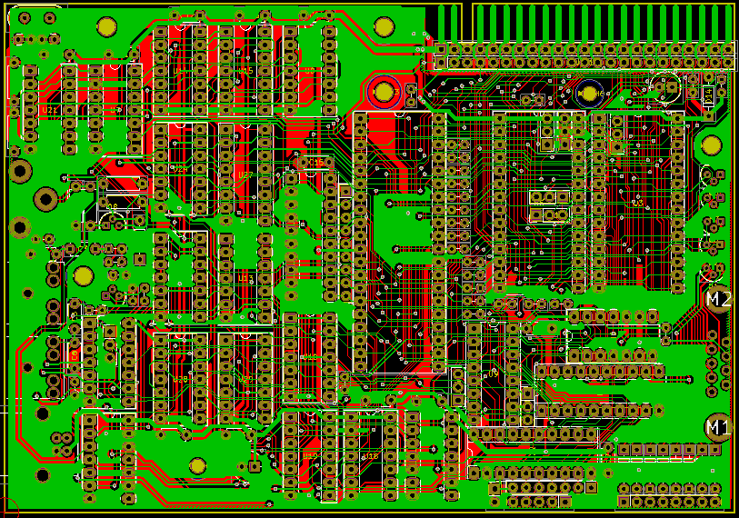
and this is the bottom layer: | |||
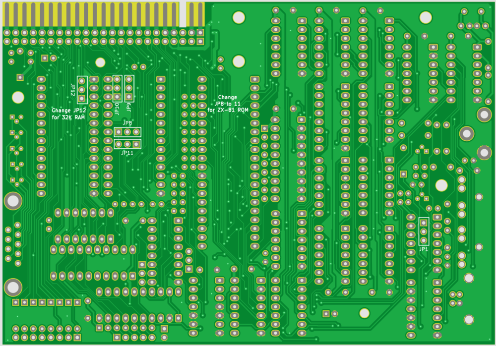
[[File:ZX81plus38 copper bottom.PNG]] | |||
I still have to work on the solder mask, (especially removing solder mask on the edge connector) and on the silk screen (paint)in the form of texts and logo's. | |||
Extra vias between top and bottom copperfill should be added wherever possible, and where possible ground traces should be added between two copperfills tightening the ground plane. | |||
== March 11, 2020 Added soldermask, and silkscreen == | |||
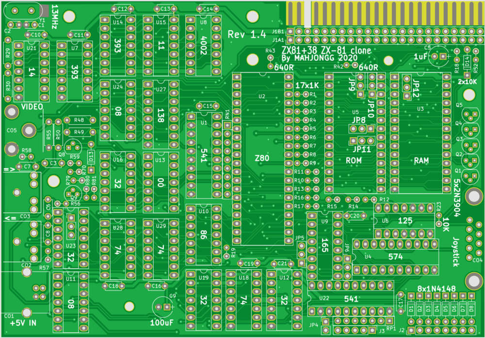
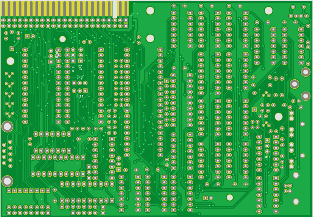
I added a soldermask, which wasn't present last week. Made openings in soldermask for edge connector, and crystal. Added silk screen text, component values etc. Enhanced ground plane with via's, and fortified +5V traces with copper planes. | |||
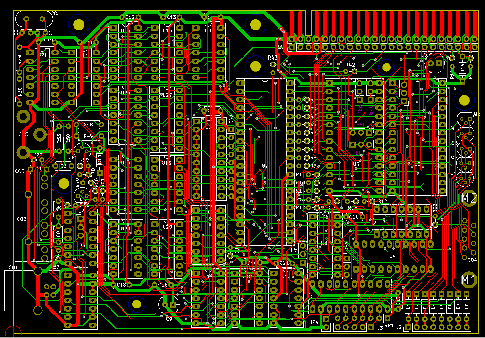
This is how the PCB will look, top view: | |||
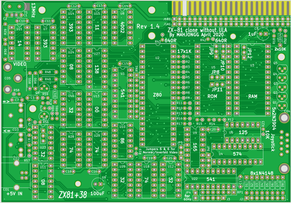
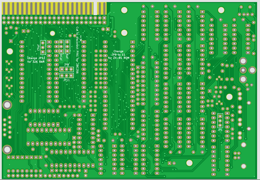
[[File:ZX81plus38 PCB rev 1,4 top view.PNG|1000px]] | |||
and bottom view | |||
[[File:ZX81plus38 PCB rev 1,4 bottom view.PNG|1000px]] | |||
== March 16, RefSpace is closed! == | |||
Still to do (when Revspace opens again): | |||
clean up pre-wired jumpers, move all of them to the bottom (as they will be underneath components when they are on top). Add the default RAM size jumper for JP12 and set it to 16K (To GND, the most standard setting) 32K is nice but non standard. Also move bottom silk screen markers to correct positions. | |||
label all jumper positions as a table on the bottom silk screen (explain their functions). | |||
Also add rectangular boxes (silk screen) around jumpers. | |||
The jumpers are: | |||
JP1, select ROM size, default = 8K alternative = 16K | |||
JP4, place to select 50Hz, open = 60Hz | |||
JP5, Invert video, default = black text alternative = white text | |||
JP6, first pixel fill, default = white, alternative = black | |||
JP8, U5 pin 23, default = A11, alternative = A12 | |||
JP9, U5 pin 26, default = A13, alternative = +5V | |||
JP10, U5 pin 20, default = nROMCS, alternative = A11 | |||
JP12, U3 PIN 1, default= GND (16K), alternative A14 (32K) | |||
== April 10, ZX-81plus38 PCB is finished == | |||
working from home, because of the corona crisis I finished the PCB layout. Made all pre-wired jumper connections accessible from the back side, and placed some descriptive text on the back about what these jumpers do. Also added a default wire for 16K/32K RAM with the default of 16K, for best compatibility with the original with a 16K memory pack. | |||
Don't forget to place the two jumpers for inverse video mode, and place default jumpers on them, in the position that pleases you, but don't forget that the real ZX-81 displayed black text on a white background. One jumper inverts the bits, another determines the "fill in color", with this setting wrong white or black stripes can appear between the letters. | |||
JP4 is normally left open, unless you are using an NTSC TV instead of the normal PAL TV. | |||
JP1 only has to change if you use a larger (than 8K) (E)PROM or OTP-ROM. | |||
When using a Atmel AT27C256R (32K) the code fits four times in the available size, I would recommend programming four identical 8K copies in the ROM. | |||
This is a picture of the final PCB: | |||
Top: | |||
[[File:Final ZX81plus38 PCB rev 1,4 top view.PNG|1000px]] | |||
and bottom: | |||
[[File:Final ZX81plus38 PCB rev 1,4 bottom view.PNG|1000px]] | |||
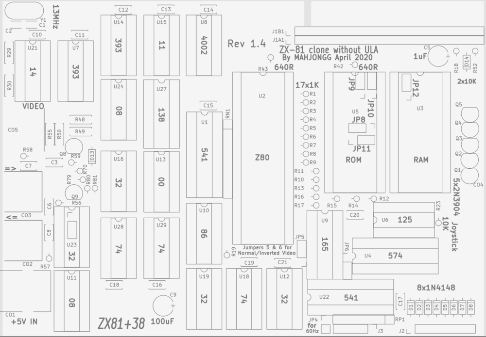
I also made a component overview drawing | |||
[[File:Final ZX81plus38 PCB rev 1,4 silk screen top.PNG|1000px]] | |||
I'm working on a bill of materials, and a final schematic (black and white .PDF) | |||
Currently I have uploaded a .ZIP with gerber and drill files to github, here: | |||
[https://github.com/mahjongg2/ZX81plus38/raw/master/ZX81%2B38%20rev%201%2C4%20gerber%20files.zip] | |||
my GitHub page is here: [https://github.com/mahjongg2] | |||
Its a bit hidden in the LICENSE.md directory, that will be corrected, and other stuff will be added, such as the BOM and KiCad files. | |||
by the way, the PCB is 142.2mm wide en 99.0mm high, you might need those dimensions when ordering a PCB. | |||
== Due to the COVID-19 crisis progress has temporarily halted == | |||
RevSpace was/is in lockdown, and working on this project from home proved problematic, but slowly I will pick up the work again. | |||
next will be the Schematic in black and white, the BOM, and a keyboard layout specific for the ZX81plus38. Hopefully I didn't do the previous keyboard with the older windows CAD software, as if I did I have to do it over with KiCad. | |||
== I managed to work from home == | |||
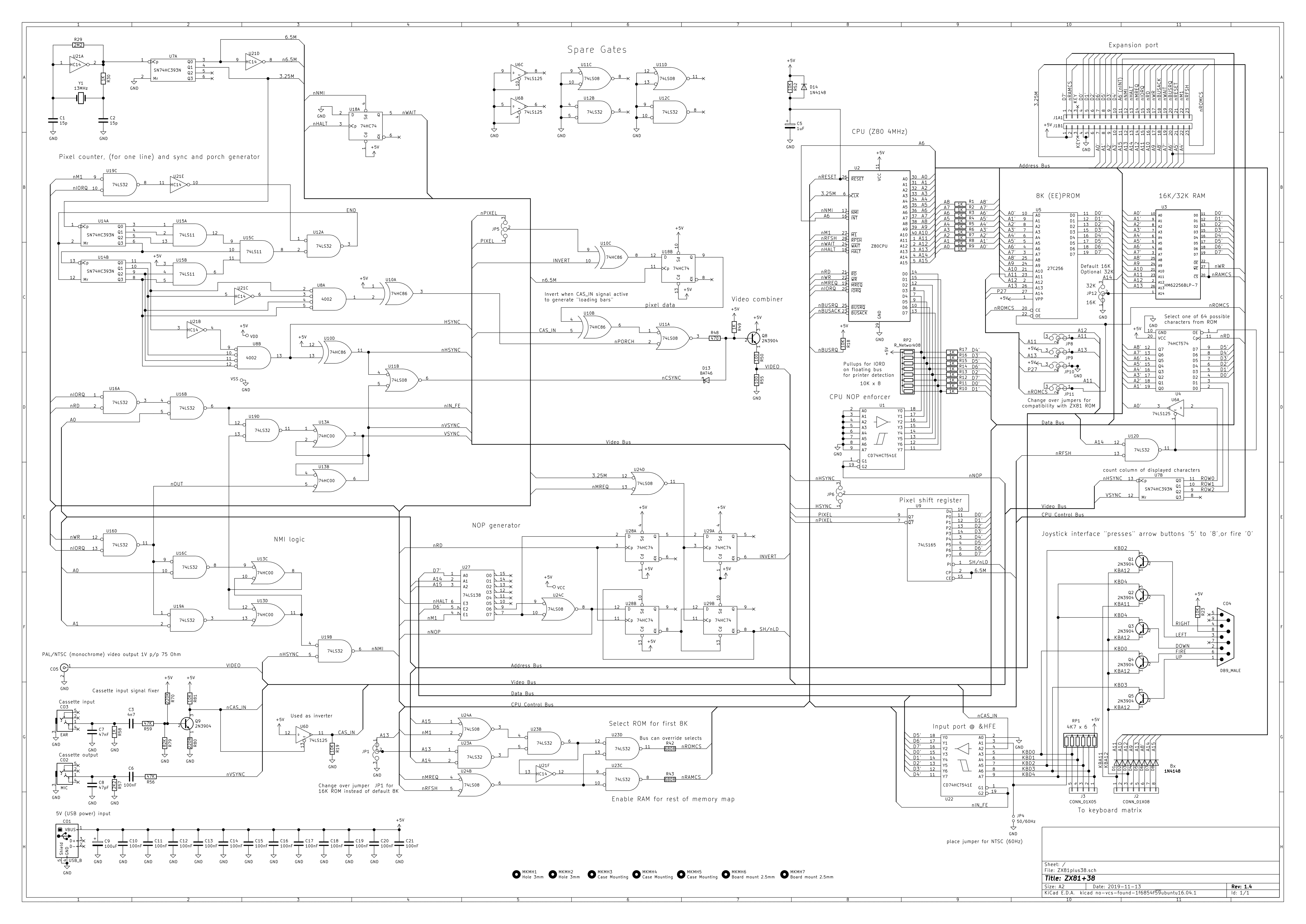
I finished the promised schematic in black and white, also found and corrected a few minor mistakes, 620 Ohm resistors do not exist in the E12 range and should be 680 Ohm, and RP2 was named incorrectly. this is the final schematic of 12 September 2020: [[File:ZX81plus38Rev1.4BW.pdf]] | |||
[[File:ZX81plus38Rev1,4BW.png]] | |||
I also finished the BOM of the ZX81+38, so now you can order the components. I used two sources for components, as neither of the to had all the components that are necessary. I used farnell and mouser as suppliers, and between them they had everything that is necessary to build this ZX-81 clone. This is the spreadsheet in open office (.ODS) format. | |||
[[File:ZX81plus38 BOM.ods]]. | |||
I will try to upload these two files to github too. | |||
== Revision 1.5 with various corrections should now be working == | |||
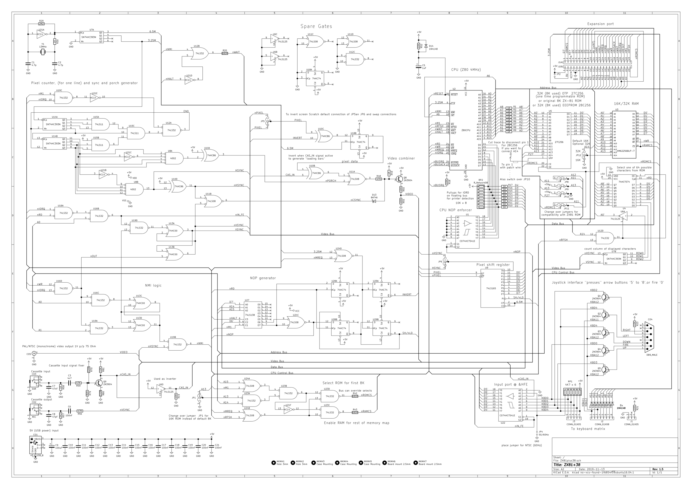
In this schematic all the reported faults and requested improvements are implemented. | |||
[[File:ZX81plus38rev1,5.pdf]] | |||
[[File:ZX81plus38rev1,5.png]] | |||
The following changes were made: | |||
# C1 and C2 of the crystal oscillator were lowered to 4.7pF | |||
# the signal n6.5M was removed, and flip/flop U18B was clocked with the non inverted clock 6.5M | |||
# the removed inverter U21D was used to build a new WAIT generator circuit in place of U18A, together with OR port U12B. the previous version did not work mainly because of the flip/flop not working as a WAIT generator. To be able to externally for the /WAIT signal low a resistor R20 was placed in series with the nWAIT output. | |||
# The RCA PSG01546 plug had a wrong footprint, and so could only be place 180 degrees rotated (not that it would work if you did). I found a replacement RCA plug that could be inserted, the CLIFF FC68391, and updated the footprint for a perfect fit | |||
# on the expansion connector I had swapped A13 and A14, so I corrected it | |||
# also on the expansion connector JB1 pin 2 was tied to +5V, but this pin was meant for +9V, so I put a jumper between +5V and this pin, so the pin can be jumpered to +5V or tied to an external +9V source | |||
# The ROM socket was designed for an OTP (one time programmable, an EEPROM without its glass erase window) and with wire links on the bottom you could (re-jumper) by scratching a track and wiring between the other pads the socket for the original ZX-81 ROM. | |||
Some users asked if I could also support EEEPROMS, and although this was already possible pin 1 (A14 on an EEEPROM) was tied permanently high, so I made it that you could disconnect Pin 1, and tie it to something else, like a switch. | |||
# i had created the option to invert the video with two jumpers JP5 and JP6, but got the complaint that if you forgot to place these two jumpers you would get no video, so I also pre-connected these two jumpers for default white screen with black letters. | |||
Its still possible to get a black screen with white letters, but you have to scratch through the default pre-connects, and add a wire link | |||
# I got asked why the keyboard wires were not simply one strip of holes with a 2.54mm pitch,but was deliberate, the previous version has three extra holes for a power LED, and a reset button, ad I had removed these. So I added three holes, and put all holes in the same raster. Its possible to have a power LED on the keyboard now. | |||
# I enlarged the mounting hole bottom left, above the text "ZX81+38"two as requested. | |||
# Jumper JP1 was wired "in reverse", but as A13 was correctly connected to pin-1 of U23A that wasn't a problem | |||
If you have a revision 1.4 PCB, you can get it working by doing three things: | |||
# Use OTP's, not EEEPROMS (which are six times more expensive anyway) and fill the 32K rom with four copies of the ZX-81 BASIC. | |||
# Remove the output of the flip flop U28A, so that /WAIT is not driven, | |||
# and replace the WAIT circuit with either the two transistor improved wait circuit from wilf ritger, or the wait circuit of revision 1.5 with an inverter and OR port | |||
# disconnect U18B pin 11 (clk) from the inverted 6.5MHz clock, and tie it to the non inverted 6.5MHz clock, closest point to connect to is pin 2 of the shift register 74LS165 (U9). | |||
Now the clone should work. | |||
== Layout ZX81+38 rev 1,5 finished and checked == | |||
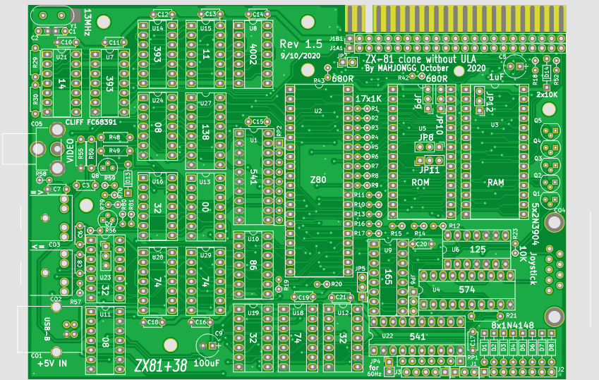
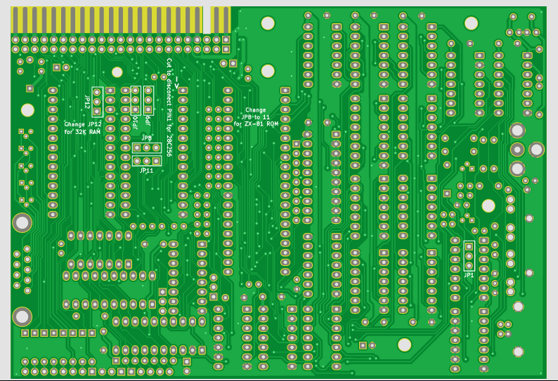
This is the new layout of revision 1.5, it has been checked for DRC errors, and this is a screenshot of how the PCB will look like true size is 142mm wide and 100mm deep, so this picture is nearly true size (depending on your monitor): Top | |||
[[file:ZX81+38rev1,5 top.png]] | |||
and bottom: | |||
[[File:ZX81+38rev1,5 bottom.png]] | |||
== A few found error makes Revision 1,6 necessary == | |||
We (the members of the microcontroller.net forum) have found another small error. The keyboard matrix uses address line A8 to A15, but A8 of this range of signals goes through a 1K resistor (signal is called A8' ) this is undesirable! Just as A9 to A15 do not go through a 1K resistor so shouldn't A8 go through a resistor, as otherwise the data-line driven by A8 cannot pull the signal to nearly ground level. and if a user presses two keys at the same time A8' can go to a wrong signal levelaffecting what the CPU reads from ROM or RAM resulting in a crash. So the layout must be changed so that A8' becomes just A8. | |||
Now started at this change which will become revision 1,6. | |||
this is the schematic, with a tiny change: [[File:ZX81plus38rev1,6.pdf]] | |||
The layout change was far more challenging, as I had to route a new signal (A8) throughout the PCB, from R1 to D6. | |||
Actually I was wrong, and the new routing wasn't actually needed, it was just that the pullups of 4K7 are just a bit too strong, and should have been 10K, with 4K7 the resistor divider created by the 1K address-series resistor, and 4K7 pullup made it that the logic level on the keyboard data line of a pressed key would not go low enough, and if you pressed a second key an illegal logic level could exist on A8' with 10K pullups this would be much less likely. | |||
Still, there is no reason to return to the old layout with A8' connected to D6, the original ZX-81 did that too (easier to layout I presume) so Ill keep this layout, only changed the schematics to a resistor array of 6 x 10K instead of 6 x 4K7. | |||
I kept the version number the same (rev 1,6) | |||
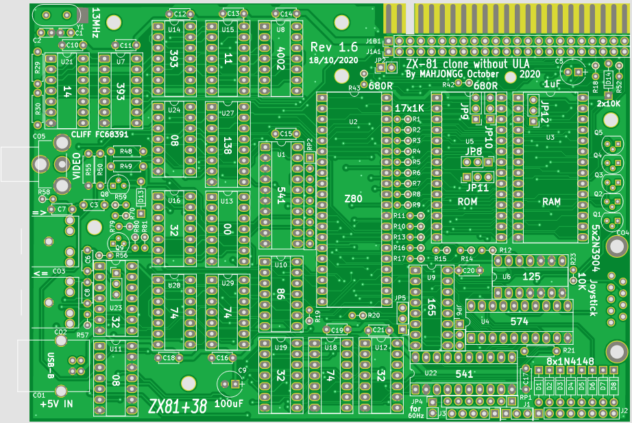
This is the new TOP side of rev 1,6 | |||
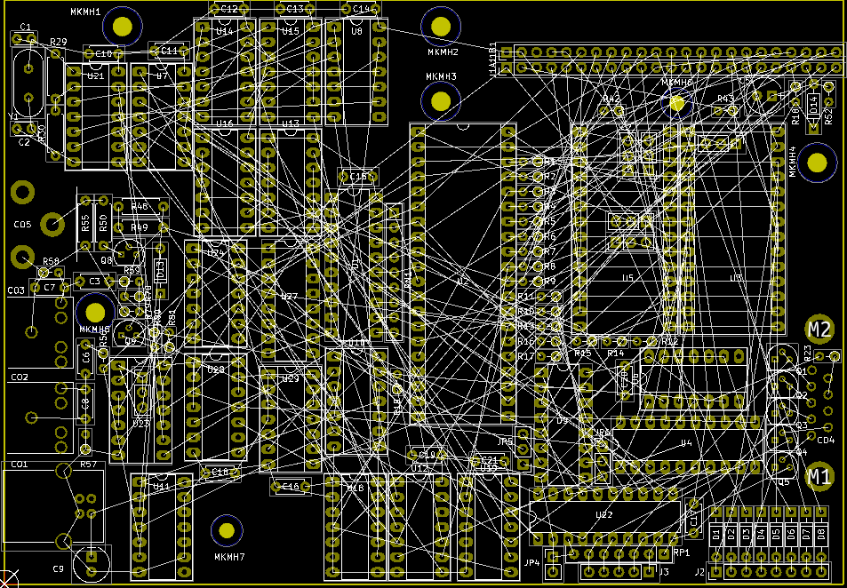
[[File:PCB PrevIew ZX81+38 rev 1,6 top.png]] | |||
and this is the bottom side: | |||
[[File:PCB PrevIew ZX81+38 rev 1,6 bottom.png]] | |||
== 11 november 2020, I received a rev 1.6 PCB, and parts== | |||
I'm now in possession of a rev 1.6 PCB, and all the parts, including a programmed (OTP) ROM, thanks to donations from persons building my ZX-81+38. | |||
Unfortunately due the revspace being in complete lockdown, I cannot build up my copy of the ZX-81+38, nor can I check if the PCB fits into the regular ZX-81 enclosure. | |||
so until revspace re-opens, (enough so that I can go there and lend a soldering iron, and check if the PCB fits) Im not able to continue building and testing the ZX-81 until say half december. | |||
Perhaps one thing I can do is designing a ZON clone board for the ZX-81+38, as I have done for the ZX-81+35. | |||
== 26 november 2020, I found a suitable soldering iron at home == | |||
I was looking for a red pencil iron I thought I had, but I cannot find it, instead I found a cheap 15Watt iron still in its blister package, I did not know I had (no idea where I got it from), but its useable and suitable for 240V (its not a 110V iron, from the CRT repair workshop I did). I also found a solder iron holder with a sponge into which this solder iron fits nicely, and a roll of suitable (60/40 solder with resin core) solder. And I also found an extension cord so I have more than one mains socket at my kitchen table. So I'm all set to start with the revision 1.6 PCB. | |||
I'm slowly recovering from my "covid recovery syndrome" sickness (which felt like a very bad worsening of my asthma) i'm slowly getting a bit more energy, in the past 5 or so weeks I could not even walk 100 meter without "blacking out" and having to sit down. Which made shopping for food very difficult, even though I practically live above the supermarket. | |||
Hopefully I will get back my energy, so I can start soldering. | |||
P.S. I went to a cardiologist to have my heart checked out, but there doesn't seem to be any problem with my heart, and the visit only resulted in a small change in my medication, and obviously in a big relief. Very soon I will be vaccinated for covid. Hopefully this will give me a bit more energy as my energy level has been very low the last half year or so. I have not done much work on my own prototype (revision 1.6 board) I just soldered about 3/4 of the sockets. Hopefully I will do some more soon. I'm curious if it works exactly as I expect it, especially if the loading bar emulation logic works exactly as I planned. Several builder have announced that the revision 1.6 now works "perfectly" (for them). I also need to get my earlier keyboard PCB, which I suspect is still at Revspace. The expectation is that many covid limitations will be lifted in a few weeks. | |||
by the way, you can find all files you need to build my clone at https://github.com/mahjongg2/ZX81plus38 | |||
If you want to communicate with me you can post in the ZX81plus38 thread I have on the raspberry PI forum here: https://www.raspberrypi.org/forums/viewtopic.php?f=62&t=254492 | |||
if it is locked for new posts (it will automatically be locked after 180 days of inactivity) click on the flag icon above the post to flag a moderator, and ask to unlock the thread. | |||
== April 17, 2022 I Produced a component placement diagram for rev 1.6 == | |||
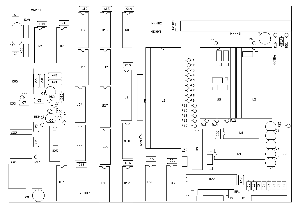
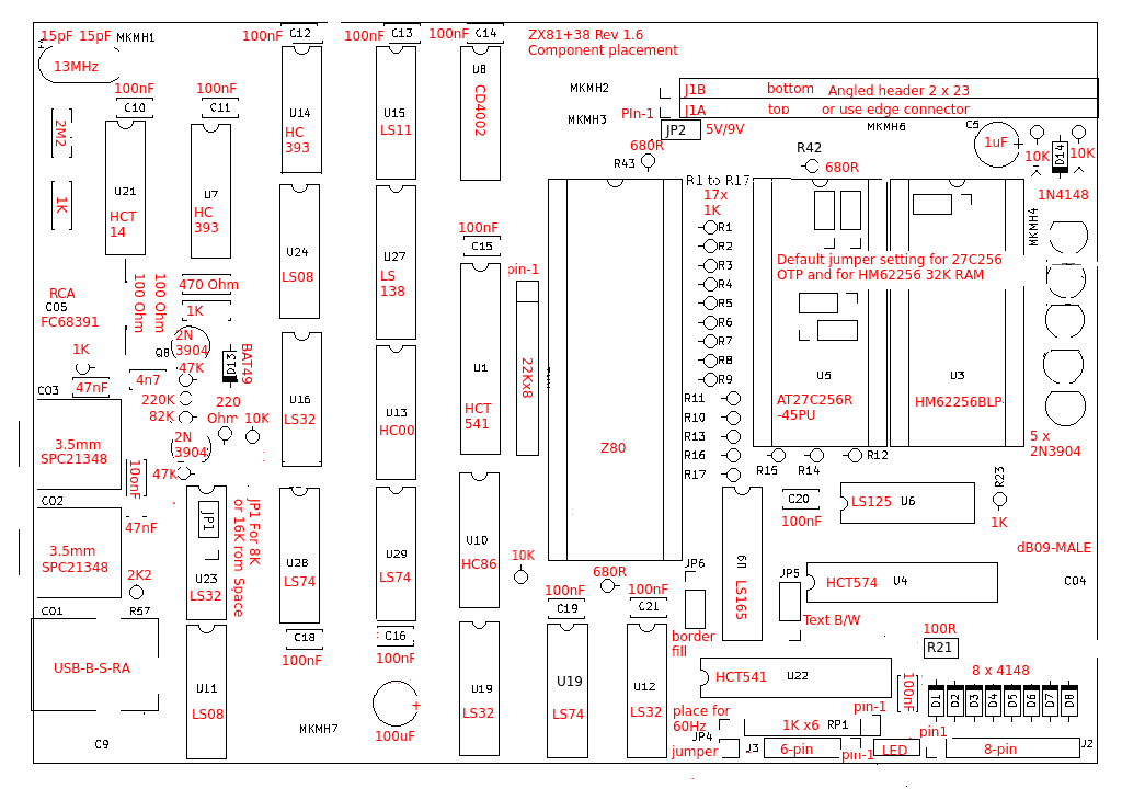
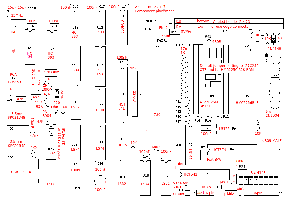
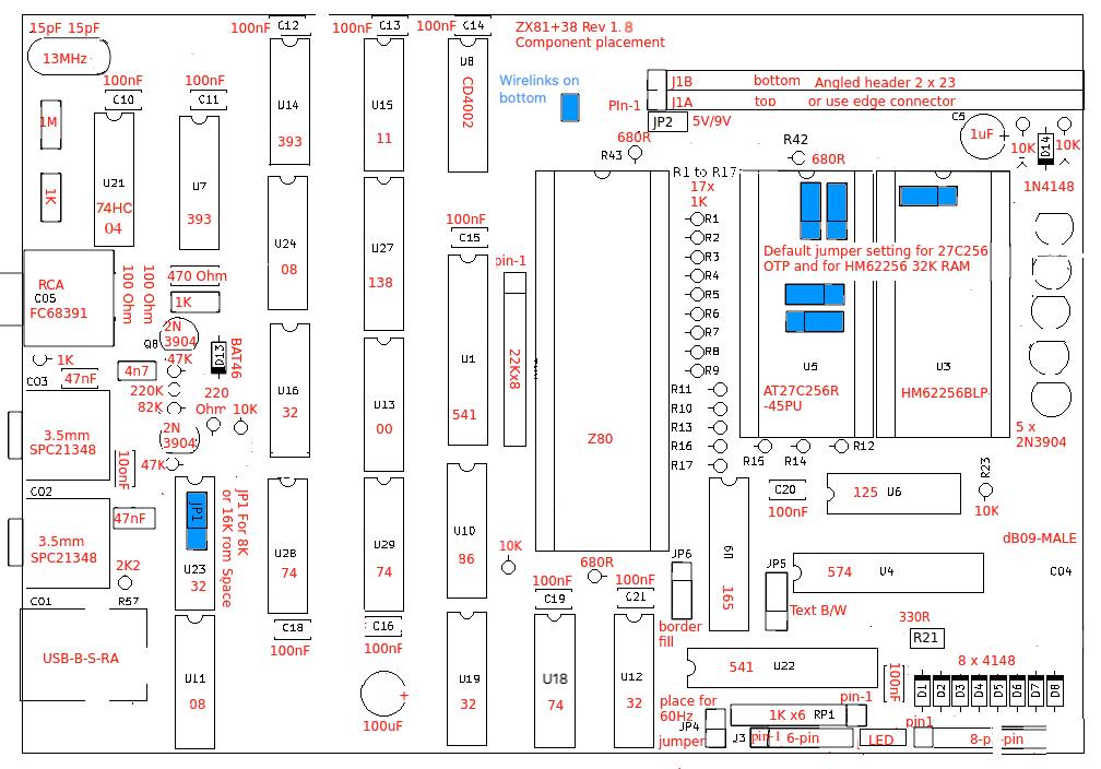
To assist building up my own prototype board, I have drawn a component placement diagram, while editing it I discovered how much this version has changed in regards to the version I used as a basis, (I think it was revision 1.4) but AFAIK this diagram is now correct for a revision 1.6 board. | |||
I will soon used it, and hopefully, if there are any problems with it I will catch and repair the errors. While doing this I also discovered a few small corrections in the Bill of material (BOM) file, and corrected those too. In the schematic a few resistors were listed as 640 Ohm, that is incorrect they should have been 680 Ohm, 640 ohm isn't a standard value, also an extra 680 ohm was inserted in the nWAIT signal. | |||
here is the drawing: | |||
[[File:ZX81+38 rev 1.6 component placement.png]] | |||
== May 3, 2022 After more than two year of covid related delay I finally re-started building my own copy == | |||
I finished soldering all the sockets and parts on my copy of the ZX81+38! | |||
I also tried powering up the board (without any IC's placed) and measured if all IC's received power, and if the polarity was OK, it was, and there were no shorts either. | |||
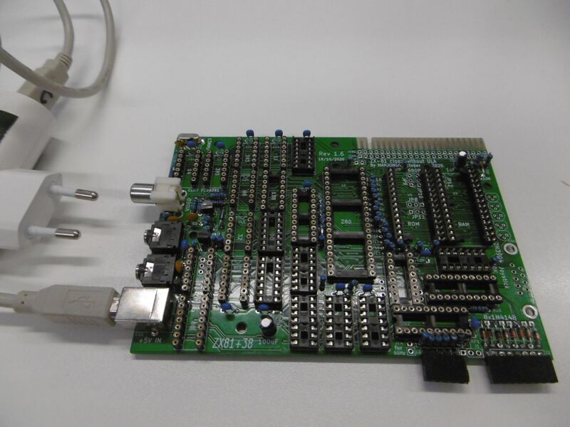
Here is a picture of the result. I have to place all IC's (I should have them), and program the EPROM (27C256R-45PU) using the REVSpace TL866II plus XGecu programmer, meaning I have to install the programmer software on my laptop. | |||
Here is a picture of the built up ZX81+38 PCB: | |||
[[File:Opgebouwd.JPG|800px]] | |||
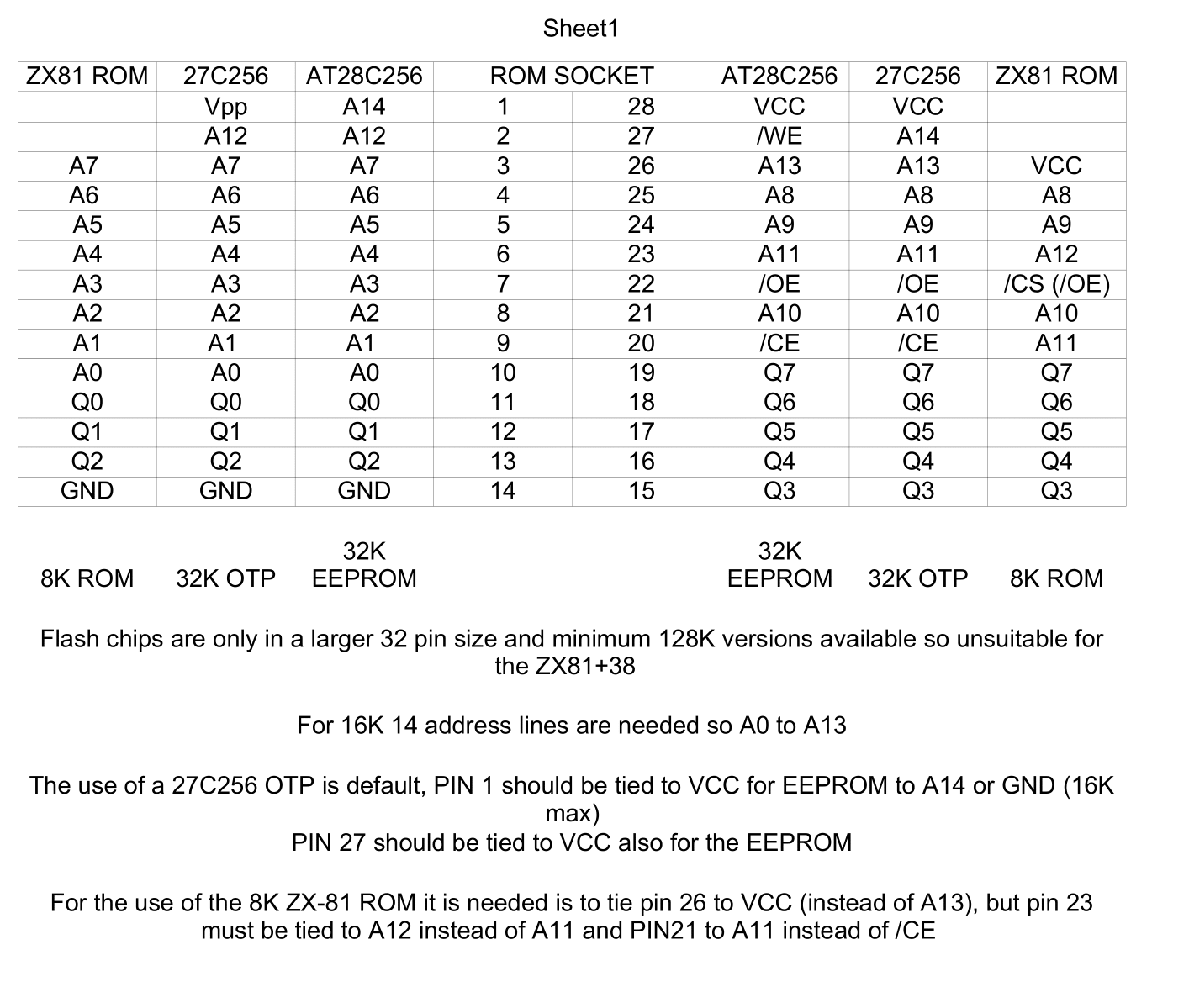
I also made a drawing explaining the thee choices of ROM's that can be used for the ZX81+38 | |||
* An original ZX-81 ROM | |||
* an 32K OTP (27C256) used as a 16K x 8 ROM, with the option to put Thomas PSG-SD card reader software in the second 8K of ROM, the default option | |||
* a 32K EEPROM (28C256) also used as a 16K x 8 ROM, same as the OTP, but useful if you expect you will need to reprogram the ROM often | |||
[[File:Rom pinouts for ZX81+38 resized.png]] | |||
reference the schematic (revision 1.6) if you want to change the wiring for either the original ZX-81 ROM, or for the reprogrammable EEPROM, for the default use of an OTP 27C256 no changes to the wiring are needed, not that changing the wiring involved cutting traces between "jumper locations" on the back of the board, and wiring the other configuration with this wires, obviously you can't install real jumpers as they would interfere with the ROM socket. Cutting and wiring is only needed for something other than the 27C256 OTP ROM! | |||
Note that there exists a 27Cxxx EEPROM that is an EPROM that is electrically erasable, the WINBOND W27C512, which is also twice the size as the normal 27C256, it needs no programming voltage and uses PIN-1 for one more address line (A15) as it is normally tied high it acts like a normal 27C256, except that the ROM content must be programmed in the top half of the memory. Alternatively you could isolate pin 1, and use another switch to switch between the two 256K halves. | |||
Also not that the latest PCB already supports a 16K "rom space" in the memory map, occupying the first 16K of address spacing, all the rest of memory space will select the static RAM, probably partly in two 16K memory mirrors.so the ZX-81 will only see 32K not 48K (with the HM62256BLP 32K SRAM chip used) | |||
== May 24, 2020 slowly making progress == | |||
I managed to get Windows 7 booting again on my laptop, but its quite a convoluted progress. I have a multi boot menu from my Linux Mint install, but when I chose windows 7 from the boot menu windows claimed "something has changed and I can't boot, please use a windows 7 install disk to fix the error" which I tried, but windows claimed not to be able to use my install disk, so I was stuck! And I still wanted to use the TL866 II plus programmer with windows (under linux there is only a command line driver, which makes using it impossible for me, don't get why there is no GUI for it!). | |||
But I found a way to start windows 7, the trick is to press enter to interrupt the standard boot up process of my laptop, then I could press F11 to start in Recovery mode, which again started the same ""something has changed and I can't boot" message but this time when I press ESC in that screen windows boots! So I booted windows, found new software for the (greatly enhanced TL866 II plus) programmer from a chinese site (if you choose the "download from local second download option it downloads an installer packed as an RAR file, so I also had to install WINRAR, and I installed some kind of HEX editor for good measure. | |||
So the programmer software was unRARed an installed which went smoothly, and I had working programming software. With that I found out that one of my two 74HC14 IC's was defective (use the 7414 options to test) that was due to me being stupid (foggy in the head) and placing it in it's socket the wrong way around, and no 74HC14 do not tolerate being fed negative 5Volt! | |||
but the other 74HC14 was fine. | |||
I have thought about why the 13MHz crystal oscillator did not work last time, even with the "good chip", and came to one of a few theories, the first is that the 2M2 feedback resistor was too large (in value), so I replaced it with a 1 Meg resistor, the second problem I could force is that a HC14 hex inverter might not like having its other five inputs floating, so I temporary fixed it so the other 5 inputs were either tied to +5V or another inverter output. next week I will test the oscillator with an oscilloscope, hopefully it will start working. | |||
I also was give three 27C512 EPROM's which the programmer said were not empty, but the donor of the chips found out these can actually be reprogrammed! they are in fact EEPROM's, not OTP's. also I was given a 28C256 by a generous german builder of my ZX81+38 (who also donated many chips and a revision 1.6 PCB). I found with the programmer this chip was filed with four copies of the ZX-81 ROM! so I had the code which I could download to my laptop from the EEPROM, and program twice in the 27C512, so it has eight 8K copies, which should work with my Revision 1.6 PCB without any modifications needed. also my 32K RAM chip tested good with the programmer. So now I have three 27C512 EEPROMs with ZX-81 code, and a 28C256, but that one needs patching the board so I probably will not need it, but as a source for ZX-81 BASIC ROM it was great. | |||
next week I will continue with the xtal oscillator. | |||
Obviously windows wanted to update first 9 updates, then after a restart (to see if I could re-boot windows without needing the installer CD) it again wanted to install again, next time I will reboot windows it will probably want to finish the install as windows always does, I hate that! It was the main reason to switch to using Linux Mint! | |||
== juni 1 2022, crystal oscilator is working! == | |||
Found out I had a defective 13 MHz crystal. Tested with a 12MHz crystal and it worked (with 1M feedback resistor, and the original 74HC14). | |||
So even with the worst type of inverter (schmitt trigger) it works, but I have tied all other inverter inputs to a stable logic level instead of floating, that initially might have had something to do with it. | |||
probably unsoldering the crystal broke it, another potential problem might be that the top of the solder pads short to the metal of the crystal, so I advise to put a piece of paper under the crystal to prevent a short. | |||
Will update schematic and BOM with the optimal IC, the "unbuffered" version of the 74HC04, the 74HCU04, which is the fastest inverter , don't understand why I chose the schmitt trigger inverter 74HC14, which is the worst possible choice, as it requires a much larger input swing, and introduces a longer delay! will update Github, also R21 is the series resistor of the power LED, which is only needed when you use a power LED (on your keyboard PCB) I suggest using 220 Ohm. | |||
So now I need to get another 13MHz crystal, and a 74HCU04. | |||
P.S. Mario "kinzi" Kienspergher wrote me that the not working crystal oscillator is almost certainly due to the use of schmitt trigger inverters, and that his experience is that it can work with 12Mhz while not at all working with 13Mhz, Jens hauslage wrote he got the oscillator working by lowering the 2M2 resistor to 1M, and replacing R30 the 1K series resistor with an 68pF capacitor, he now has the inverted K cursor and is working on the keyboard now. | |||
== juni 7 2022, still have crystal oscilator problems for my own copy == | |||
Update, found out my 13MHz crystal is absolutely defective, tried to use some other inverter IC's but (opviously if you think about it) none of the ones I tried work (74LS04 and 74L04, obviously I need a CMOS inverter), so the problem stays that I need to buy a new 13MHz crystal, and a 74HC04 or 74HCU04 which is difficult for now because I no longer have access to many sources such as Farnell (without working for a company). | |||
I will keep trying. found a 13.025 MHz mini crystal I might use. | |||
== juni 22 2022, got a free Xtal and 74HCU04, Finished Revision 1.7 == | |||
will try the new crystal and 74HCU04 next time when I'm at Revspace. | |||
I also got An I/O expansion board (8 input and 8 outputs) from the same ZX81+38 enthousiast that gifted the Xtal and 74HCU04. | |||
In the meantime I got a few tips and requests from him which led to me creating revision 1.7: | |||
The changes (relative to 1.6) are: | |||
*Changed footpad of crystal oscillator to a footpad that supports both PTH and SMT crystals. You do need an isolator between crystal case and pads when using a crystal with leads if you must use it as a pin through hole crystal, to avoid shorts. When using an SMT crystal, it will come with a plastic base, and shorts are not possible simply solder the wires to the pads from the top side. | |||
*Changed R29 to 1M, U21 to 74HCU04, also changed RP2 to 8x22K and changed the series resistor R21 to 330 Ohm (was 100Ohm) all as the latest BOM tells you. | |||
*changed the default JP1 jumping so that there will be 16K of ROM-space, not 8K, if you want to use four separate 8K images then switch JP1 back to 8K ROM-Space. then you can use two switches to drive A13 and A14 with switches, after having disconnected the pre-wired trace between jumpers JP9 and JP10. | |||
*The same user that gifted me stuff also remarked he had to twist the 5-wire data lead (foil) because J3 was reversed in orientation, this must be the last of many keyboard wiring errors I have made, so I need to also create a specific ZX8138 keypad with wiring 100% compatible with a real ZX-81. note that this means the keyboard data lines on the ZX81+35 are inverted too, I will do no changes to ZX81+35 anymore, sorry. | |||
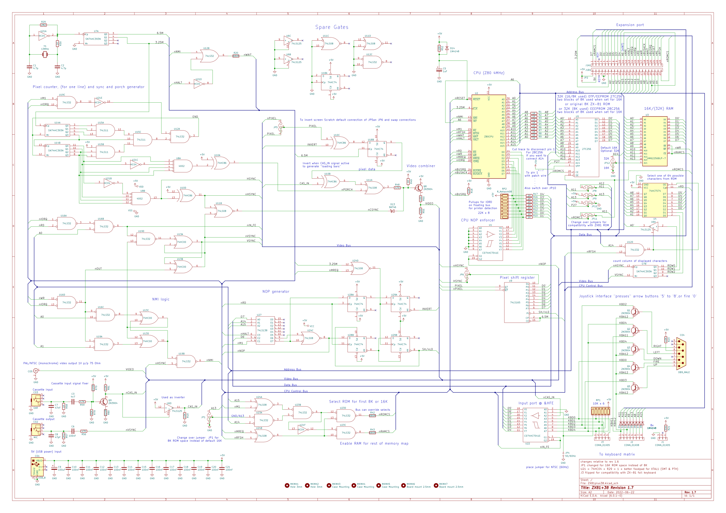
The new schematic as .PDF [[File:ZX81plus38 Rev 1,7.pdf]] | |||
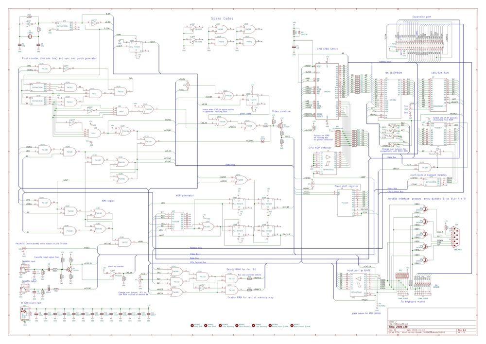
[[File:ZX81plus38 Rev 1,7-resized.png]] | |||
and updated placement file | |||
[[File:ZX81+38 rev 1.7 component placement.png]] | |||
== It happened I uploaded all ZX81+38 revision 1.7 files to GitHub == | |||
Updated files, are the Production files (.zip) with all the gerber an drill files to create the PCB, a schematic (in monochrome) of revision 1.7, and a picture of the updated placement file. | |||
The earlier updated BOM files is compatible with revision 1.7 and now also has more sources listed for components. To top it all of I uploaded the 8K ROM file for a ZX81 (clone) which is legal as the ROM was freed to the public domain. I'm still planning to release the full set of KiCad files (including extra schematic and footprint libraries) to GitHub in the near future. | |||
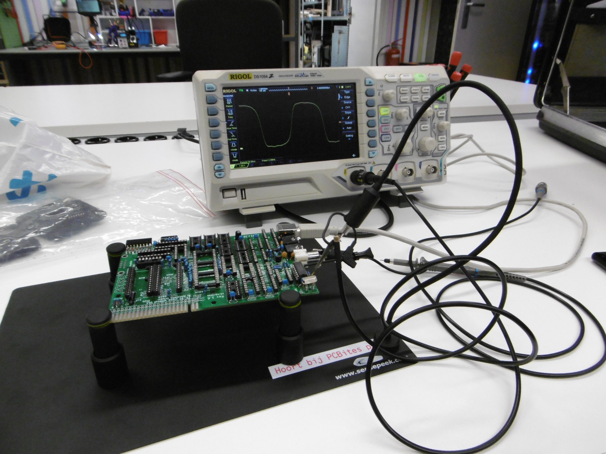
== June 29, 2022 The crystal oscillator is working! == | |||
[[File:P1030120.JPG]] | |||
I am using a 74HCU04, but no doubt a 74HC04 will work as well. I now have soldered the crystal directly to the board without sockets, and used a small piece of Kapton | |||
tape to isolate the metal body of the crystal from the pads below. | |||
== July 6, 2022 I made an observation while building up my copy of the ZX81+38 that shook me == | |||
I made a (for me) stunning discovery, as I said earlier I derived the ZX81+38 clone from my fully working ZX81+35 clone, which was built up from SMT (surface mount) IC's and in it I exclusively had used 74HC logic, even for the dual four input NOR gate the 74HC4002 which is actually a CD4000 family chip. And certainly the crystal oscillator should not be the wrong kind of logic, initially it was a single-gate CMOS logic unbuffered inverter the SN74LVC1GU04 why I replaced it with a 74HC14 I will never know. So when I read complaints that I had "mixed up logic families" I was initially unconcerned and thought that maybe I had replaced some 74HC ic's with 74HCT ic's, because a DIP version of some IC's were easier to get in 74HCT logic than in 74HC logic, and in my mind not a single 74LS family chip was used. But that illusion was shattered when I was building up the board using my self made component placement drawing and I saw many IC's being listed as LS logic! That is one reason why you will normally not release a design before you build up and test it successfully, as in that stage you are bound to find silly mistakes like that. | |||
Shock-horror how could this be, and why didn't I noticed this obvious error before, I checked the BOM, and indeed there too I noted that LS logic, not HC logic was often used! | |||
Now I have no doubt that HC(T) and LS logic CAN BE MIXED, in a 5V powered design, but as I said I did not deliberately changed any HC logic family IC to an LS IC'! | |||
Somewhere something must have gone wrong for this to have happened! | |||
I assume the fault occurred because I re-drew the schematic in KiCad, for my original (paper) ZX81+35 schematic and I remembered from that conversion project that not all IC's I needed where in the KiCad library in the form of DIP 74HC logic IC's, so sometimes I was forced to use to use the 74LS DIP library, and change the logic type (IC label) to 74HC from the original 74LS logic label, in that process something must have gone wrong! All the places where I deviated from the 74HC family and the labeling was changed back to 74LS that is in error! | |||
As the BOM was derived from the schematic, and the build up diagram was derived from the silk screen diagram and the BOM it contains the same errors. | |||
But again, this doen't mean it won't work, it should work, only drawing a bit more current than it should. As I said before I received news that someone had built u this clone with IC's he had on hand, which where military LS logic (54LS logic) and it worked fine. But this does explain why observant copyists of my design noticed the mix of logic, which I completely failed to detect. | |||
I want my designs to be perfect, so I will correct the schematic, the BOM, and the placement diagram. | |||
Another observation I also made is that sockets with machined (round) sockets are very bad at accepting imperfect IC's, so I sometimes needed half an hour to minutely straighten out IC pins, as the socket otherwise would not accept them. Recently I saw a youtube video where a retro-computer repairman repaired an oddly build up C64 by replacing its mixture of sockets and he remarked that he much rather used dual wipe sockets because machined pin sockets are notoriously bad a making reliable contact when a bit of the pins of a DIP IC was cut off, and that dual-wipe sockets were not like the cheap single wipe sockets, but were in fact even better than machined sockets. So please do yourself a favour and use dual wipe sockets not machined sockets. | |||
== July 10, 2022 updated rev 1.7 schematic, Gerber/drill and placement drawing == | |||
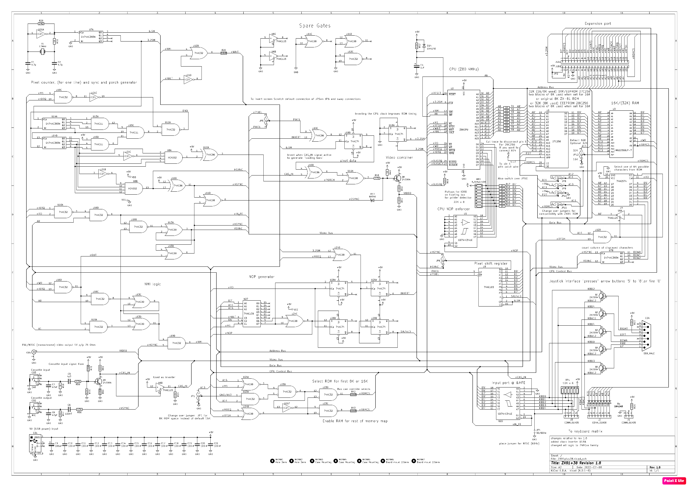
The new schematic rev 1.8 as a .PDF | |||
[[File:ZX81plus38Rev1,8.pdf]] | |||
And as .PNG picture: | |||
[[File:ZX81plus38Rev1,8.png]] | |||
The new placement file, with only HC logic: | |||
[[File:ZX81+38 rev 1.8component placement.png]] | |||
== July 13, 2022 tested my copy of the ZX81+38 == | |||
I had a short time to test my copy of the ZX81+38, short because I had to make sure the TV I used was capable of accepting a composite video signal. To do that I used my smallest NES in a joypad, and I concluded the TV produced (only) a monochrome video picture. | |||
I had little time because I came in late at Revspace, and my first priority was to replace the CR2032 battery in my recently rediscovered Dreamcast, which I didn't knew I still had. But after ten years of inactivity its battery was dead. So I opened it up, and found that the battery was soldered to a PCB, without a battery holder. But I found pieces of metal with which you can create a battery holder, if you solder it to a PCB. After some thought I found a piece of dual sided clad-board, which I could cut to size and solder to the metal, then a few wires could be soldered to both ends of the dual sided board, and I had 3.3Volt between a red and a black wire. I soldered the wires to the removed remains of the battery, and had opened the solder holes. After that I could use some dual sided sticky tape to hold the battery in place. I tested the dreamcast and my replacement battery worked. I realistically had 15 minutes left, so I decided to do a quick test of the ZX81+38, unfortuantely the result was disappointing an all black screen! | |||
No video at all!. Its not what I had hoped for, but I don't even know if the EEPROM was programmed, let alone programmed with copies of the ZX81 ROM code, so next week I will start testing what is wrong. | |||
== July 14, 2022 Updated the layout with correction of NPTH holes and USB connector positions == | |||
With help of a real ZX81 PCB, and the enclosure of a real ZX81 I could check if all the non plated holes (for screws) were in their correct positions. I found that many holes were between 0.5 and 1.5mm from their correct location, and managed with a calliper, and ruler to find aberrations, and correct them. I also moved the USB connector o.7mm toward the audio connectors, so the square type-B USB connector could be inserted while the PCB was mounted in the original case, without having to cut away any plastic from the enclosure. I generated updated gerber files, which I will upload to GitHub after checking them with a gerber viewer. | |||
== July 15, I have an idea why the first test didn't work == | |||
It literally came to me in a dream that I had forgotten to remove the patch wiring I used to keep all other 5 inverters from U21 having an unstable input level. During my quest to get the oscillator working I tied all other five 74HC14 inputs high, or to another output, and I had forgotten to remove this patch, this completely explains why, with the patch, the ZX81+38 cannot work. | |||
There is no guarantee the clone will work when I remove the patch, but I have high hopes this was it. | |||
== July 19, That wasn't it == | |||
Well I removed the patch wiring from U21, but afterwards, I still only got a black screen. So I used the MiniPro eprom programmer and checked if the EEPROM I used (W27C256, which can be electrically erased) was indeed filled with the 4 x ZX81 ROM code, which it was! So I used the same Minipro to also check all the HC logic chips (other logic like LS and HCT will be replace, so no need to test these) and I found a defective IC, a 74HC74, the one with the broken off leg, unfortunately I didn't have a replacement only a 74LS74 but with it the zx81+38 didn't work either (Im' still unsure the monitor I'm using is able to display the monochrome PAL signal that my clone is outputting, but it worked (with a monochrome picture) with my many NES in a joypad) which may or may not mean anything. | |||
I have to replace all non HC logic with HC logic, which means I need to buy : | |||
* U15, 74HC11 | |||
* U11, U24, 74HC08 | |||
* U27, 74HC138 | |||
* U12, U16,U19 74HC32 | |||
* U6, 74HC125 | |||
==July 23 2022 JP1 has become unchangeable in rev 1.7 == | |||
heard about a layout problem around pin 1 of U23, because its now connected directly to GND, the copper fill has become a problem, and it has become nearly impossible to set JP1 to 8K ROM-space. | |||
I will fix this in the still unreleased revision 1.8 gerber files. New idea is to surround JP1 with A13 traces, so the copper fill will not become a problem. | |||
== July 26, 2022 Updated all revision 1.8 files on GitHub == | |||
including new placement, BOM, schematic, and production files, removed all older files from GitHub. I added more reichelt order codes, as my replacement HC logic IC's were all ordered from reichelt (mouser didn't have everything), as ordering from Farnell has become impractical, reichelt is cheap and had everything I needed, and Sinuss (farnell for private customers) doesn't have everything and doesn't use Farrell ordercodes anymore. | |||
I ordered: | |||
* 2 x 74HC08 | |||
* 1 x 74HC11 | |||
* 3 x 74HC32 | |||
* 1 x 74HC125 | |||
* 1 X 74HC138 | |||
Delivery in 3 days, cost less than 11 euro | |||
== August 3, 2022 bad luck, I'm missing one HC IC == | |||
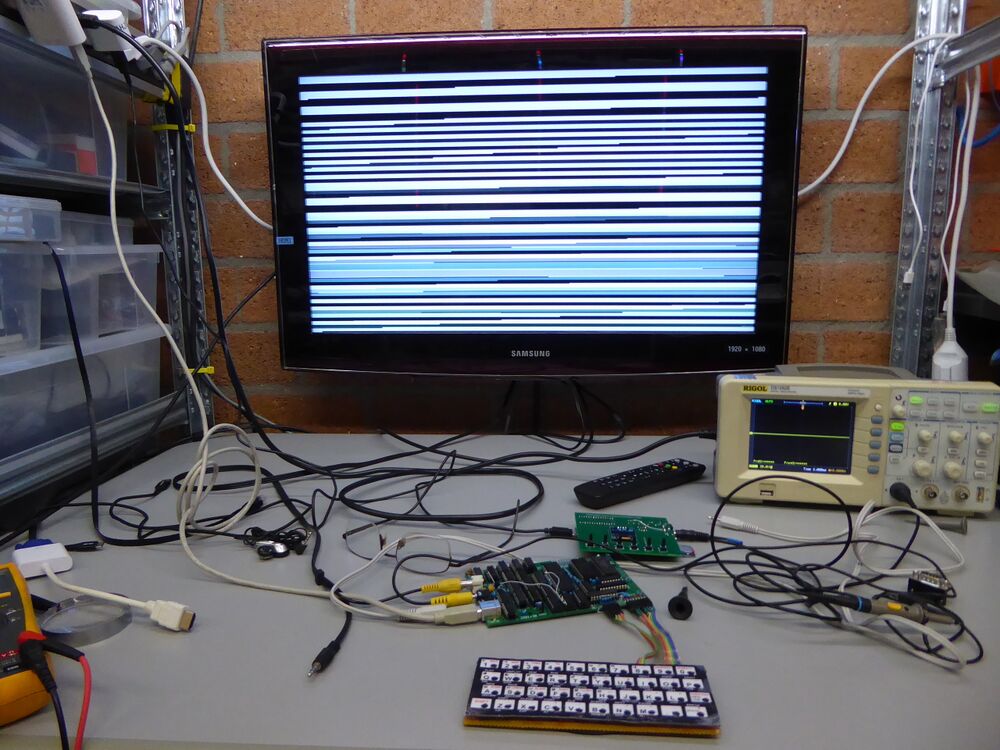
I ordered one 74HC32 too many, but I'm missing a 74HC74 I need three, but only have two and a left over 74HC32. I tried the 74LS74 in any of the three positions where it is used, namely on positions U28, U29 and U18, but none of these worked, but on all three positions a 74LS74 resulted that on a monitor with composite input the screen became a stable white with a thin vertical black stripe. | |||
I tried my ZX81+35 on the same monitor, and also got the exact same white screen with a black stripe, but the ZX81+35 worked and displayed the inverse K with a white K in a black square. Looking at the schematic it's quite logical that in none of the positions a 74LS will work, I really need one more 74HC74. | |||
I made a picture one of the ZX81+38 with one LS instead of HC logic chip and you can see the monitor shows a white screen, so sync does work, only thee are no black pixels, which is logical. I will order the missing 74HC74 chip. you can see the picture on the main page, in the top banner pictures. | |||
I have very much bad luck, or perhaps itś that I have "long covid", and I'm too fuzzy in my head. I don't normally make such mistakes this often. | |||
I also normally have much more energy and drive. | |||
I Have looked here everywhere for a 74HC74 but its just not here. hopefully soon I will have better news. | |||
== August 10, 2022 its working, but have yet to connect the keyboard == | |||
added the missing 74HC74 and at first I thought it wasn't working because I did not see the reverse K, but that is just because the ZX81 takes some time to check the memory, if you have much of it. So after a few seconds the keyword cursor, only it was just a black rectangle. I thought that would only be the case when the EEPROM would be too slow but I used a Winbond W27C512-45Z which is very fast (45nS) . but it might be so that the EEPROM is also faster in releasing the output data. | |||
So I patched my (rev 1.6) board with the CPU clock inverter patch, using U18, and that worked! | |||
I got the K prompt! | |||
I used a DuPont wire to connect one address line to one data line, and the ZX81+38 reacted, see the picture here: https://revspace.nl/kiekjes/view/20220810/P1030221.JPG | |||
So my next job is to wire my prototype keyboard to this ZX81+38 clone | |||
== August 22, 2022 Tests reveal joystick logic not working == | |||
One of the builders of my ZX81+38 revealed that the joystick port on my ZX81+38 wasn't working. Comparing the joystick logic with the one used in my ZX81+35 revealed that there were some differences, firstly the current limiting resistor that limited the current flowing in the common switch node on pin 8 of the DB-09 port was changed from 1K (limiting the current flow into the base of one (or more) 2n3904 transistors to 5mA to 10K, just 0.5mA). That is one possible problem, but the more obvious problem was that originally each base of one of the five transistors had a 10K pulldown resistor to GND, and especially the lack of these resistors made that the joystick interface didn't do what it supposed to do, that is converting the joystick action to "pressing" the relevant keyboard buttons for the four arrow keys 5,6,7, and 8 (left, down, up, and right, and the fire button 0. with the 10K current limiter changed to 1K, the interface still did not work, but adding the five 10K resistors did work!, and that means a substantial layout change is needed to add five 10K pulldown resistors. | |||
As we are now at revision 1.8 that means this will become revision 1.9 and is hopefully the last major layout. | |||
I will change the schematic, layout, BOM and placement diagram, publish the schematic here, and the schematic plus all other changed files and a new KiCad file (reduced to only what is needed) to GitHub. | |||
Looking at the available space on the board I decided to use a 5 x 10K resistor pack would be the logical solution. it fits between the RAM chip and the 2N3904 transistors. such a resistor network is available from Rechelt for seven eurocent! | |||
== August 23, 2022 Repaired joystick logic in revision 1.9 == | |||
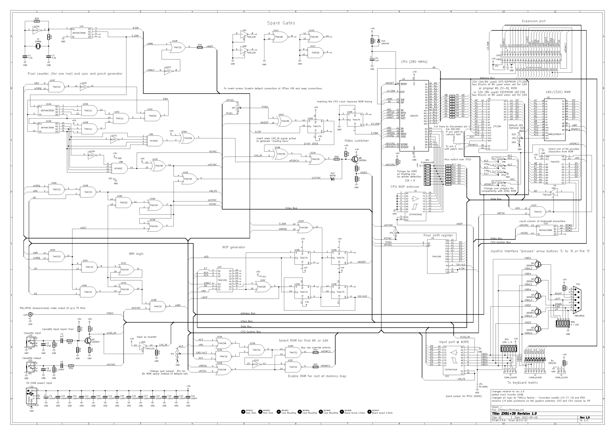
here is the revised schematic for revision 1.9: | |||
[[File:ZX81plus38rev1,9.pdf]] | |||
[[File:ZX81plus38 revision 1.9 schematic.png|2000px]] | |||
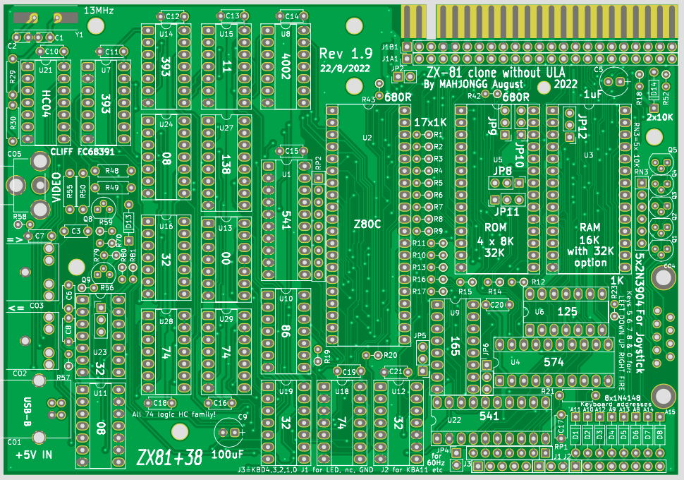
and the PCB preview (top): | |||
[[File:PCB Preview ZX81+38 rev 1,9 top.png|970px]] | |||
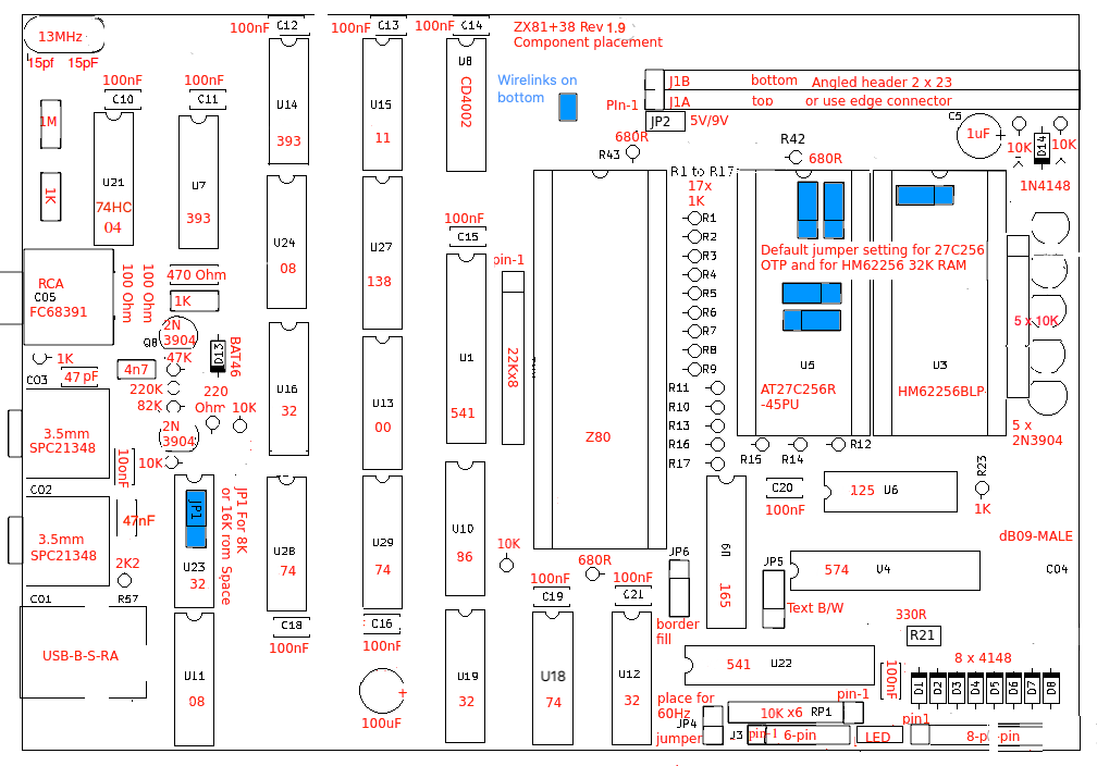
and here is the new placement drawing for revision 1.9: | |||
[[File:ZX81+38 rev 1.9 component placement.png]] | |||
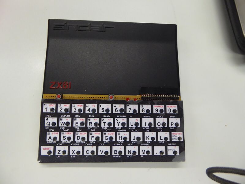
== August 23, 2022 Modify prototype keyboard to fit on top of ZX-81 == | |||
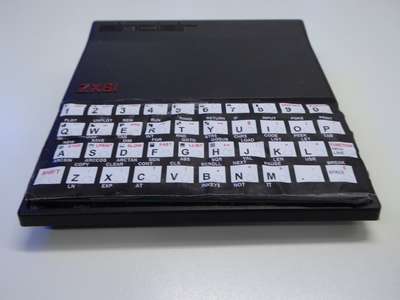
also I'm busy with modifying my old prototype keyboard for my ZX81+35 so that it works as a replacement keyboard for the foil keyboard of a real ZX-81 | |||
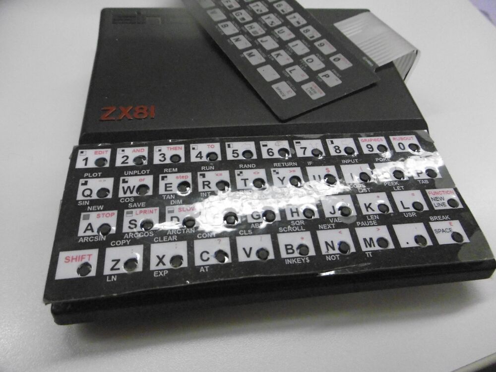
The size of the keyboard is almost exactly right, only I have added reset buttons, and two LED, and the edge connector sticks out a lot. see: | |||
[[File:ZXkeyboard on top of ZX-81.JPG|800px]] | |||
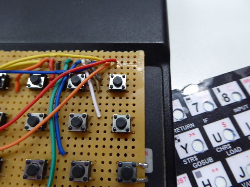
so I will remove these parts and wire two flat cables directly to the keyboard PCB. | |||
After removing the connector, I tried and found that I need two more stripboard rows. | |||
[[File:Cut one row more is needed.JPG|800px]] | |||
So I removed the wires and removed two rows of strips, leaving one row of holes over, just enough. | |||
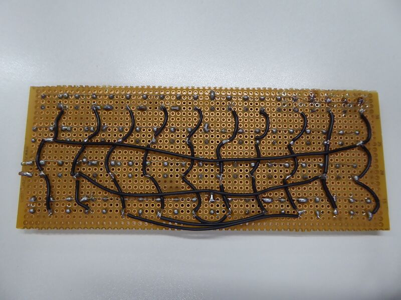
afterwards, you can see the remaining matrix wires on the back: | |||
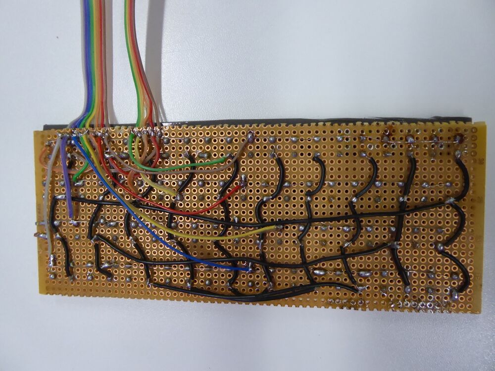
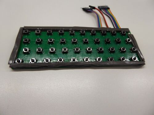
[[File:The back of the in height reduced keyboard PCB with matrix wiring.JPG|800px]] | |||
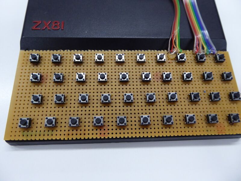
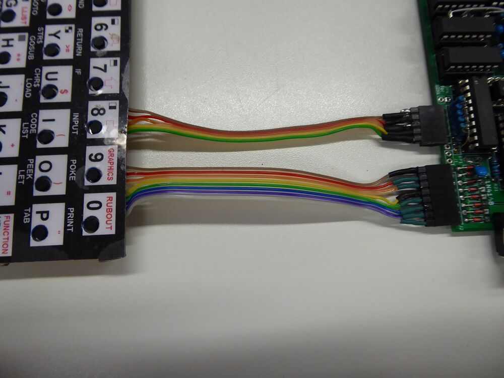
I wired the rainbow colored data and address cables to the board, on the back of the board the signal wires must still be connected to the correct rows and column matrix wires, with the same color wires. | |||
[[File:Keyboard with rainbow coloured cablels.JPG|800px]] | |||
As you can see the keyboard PCB now fits on the ZX-81, and the cables will fit through the slit in the case. | |||
next job will be to wire the matrix connections to the 5 and 8-wire cables. | |||
== Sunday August 28, 2022 Started designing the ZX81+38 Keyboard PCB == | |||
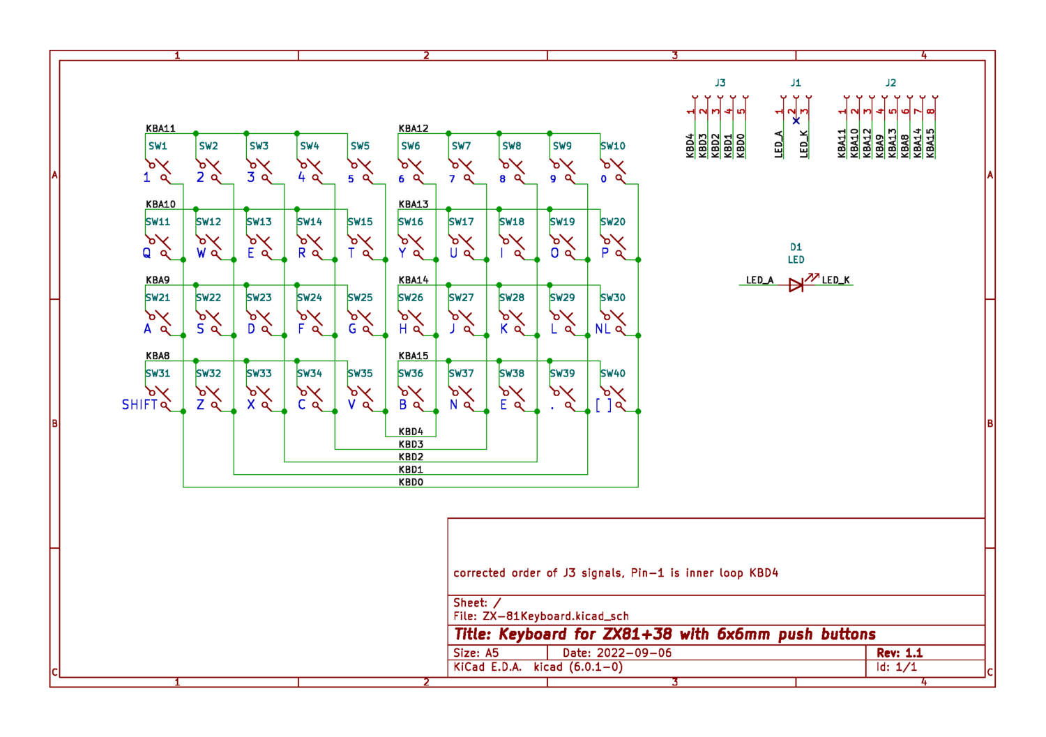
Here is already the schematic: | |||
[[File:ZX-81Keyboard color.pdf]] | |||
[[File:ZX-81Keyboard color.png|1500px]] | |||
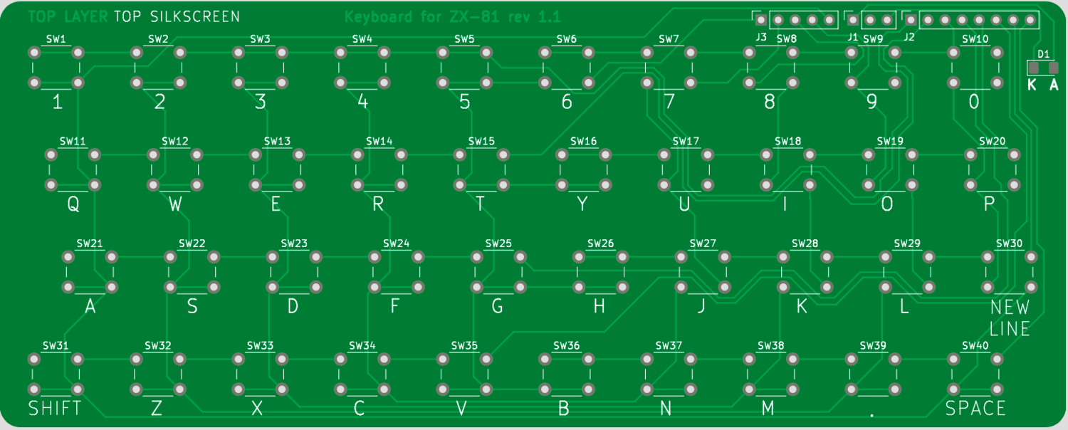
here is a preview of the PCB: | |||
[[File:ZX81+38 keyboard PCB preview.png|1500px]] | |||
This PCB is a single sided PCB, with only copper on the top side. The 40 pushbuttons are inserted on topside and also soldered to the pads on topside. | |||
the flat cable is inserted from the bottom, and soldered on the top. cut the pins on the bottom side off as close as possible to the PCB, and mount the PCB in the indentation with dual sided (carpet mounting) tape, but don't place tape over the flat cable connections. | |||
If the flat cable is thicker than the carpet tape, you might need to carve out some plastic to make place for the flat cable. | |||
print out the keyboard overlay drawing, laminate it and punch out round holes through with the keyboard stems will go with a paper punch and a hammer while placing the laminated paper on flat wood. | |||
The holes should fit exactly over the buttons stems. | |||
== Tuesday August 31, 2022 keyboard works! == | |||
Still I had expected the need to twist the data cable, but for some reason that isn't necessary, which means that because I'm using the rev 1.6 board that I expected that the order of the datacable should be wrong! | |||
At home I have a real keyboard, so I can finally check what the true order should be. Maybe this means the keyboard PCB is wrong! But I will go to the bottom of it! | |||
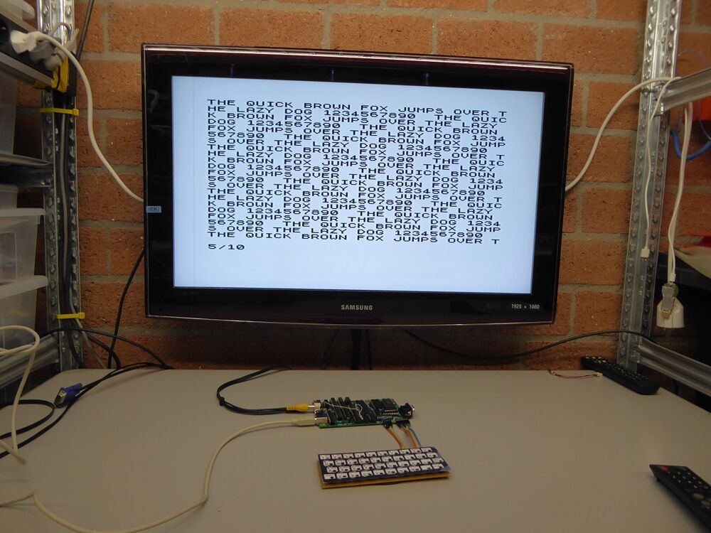
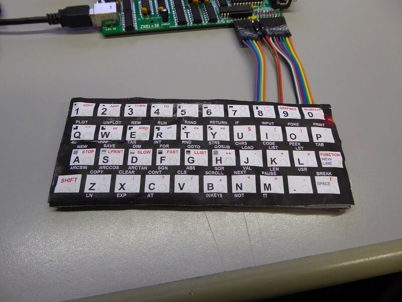
here is proof that the keyboard now works! | |||
[[File:Success!.JPG|1000px]] | |||
you can see that I didn't twist the cable. | |||
[[File:Cabling.JPG|1000px]] | |||
this is how I wired the keyboard data and keyboard addresses to the keyboard matrix. | |||
[[File:Wiring.JPG|1000px]] | |||
you can see the green wire is connected to KBD4 the inner loop (the two inner columns). | |||
and the brown wire (KBD0) is connected to the outer two columns. | |||
I tried to wire my prototype keyboard identical to a real ZX-81 keyboard, perhaps I made a mistake somewhere? | |||
I can measure on the tape ends of a real zx-81 keyboard how it is wired. | |||
== Tuesday september 6, 2022 found error in keyboard == | |||
When I tried my prototype keyboard, which I assumed was wired exactly as a real ZX-81 keyboard foil I discovered that I did not have to twist the keyboard data (5-wire) connector, which was unexpected as I'm using a revision 1.6 PCB, and it should have a twitched keyboard data connector. So I investigated further, I desoldered the keyboard (molex) connectors from a real ZX-81, so I could press-fit the foil ends of the real keyboard foil of a ZX-81 and attach it to my revision 1.6 version of the ZX81+38 to check. I also tried to get more information on how the keyboard foil was wired internally. I found a youtube film where the internal wiring was visible, and I concluded that KBD4 (connected to the inner two keyboard columns (keys 5,6,T, Y, G, H, and B,N ) were connected to the most left side of J3 (Pin-1), and that indeed meant that I wired my prototype keyboard wrong. I corrected the schematic and the layout of the keyboard and updated the revision to rev 1.1, see schematics above, and the preview of rev 1.1. | |||
== Thursday september 8, 2022 released keyboard PCB design files to GitHub. == | |||
I released the schematic (revision 1.1), the production files for the PCB also revision 1.1, and a new BOM I made for the keyboard. I also included the keyboard overlay drawing (.pdf) so you can print it out and laminated (or spray it with transparent lacquer) punch the holes in it for the button plungers (now somewhat longer ones) and cut it to size (after glueing it to the top of the buttons). | |||
I finally am confident enough about the wiring, so its 100% compatible with a real ZX-81 keyboard. I also uploaded the KiCad files. and gave an explanation how best to use a 1.27mm pitch flat cable, by removing 1 cm of every even wire in the cable, so the pitch of the remaining wires will be 2.54 mm. The buttons should be soldered on the top side, flush to the keyboard PCB, so that the forces from pressing on the buttons will not rip-off the PCB pads and traces. | |||
And you should cut the leads from the button very close to the PCB, so the PCB can be glued tightly to the indentation on the to of the case meant for the foil keyboard, it should fit correctly, with the keyboard overlay sticking a bit out over the PCB, but can be cut to exactly the edges of the ZX-81 case. | |||
The revision 1.1 keyboard will be 100% compatible with a real ZX-81, and revision 1.8 (or later) of my ZX81+38. | |||
with that I conclude that the status of the ZX81+38 is now Completed, and I can now start of the PSG + SD-card expansion board for the ZX81+38. | |||
== Saturday september 10, 2022 Corrected error in silkscreen text of keyboard == | |||
The keyboard is now revision 1.2, but electrically nothing has changed and the same BOM can still be used. as well as the gerber files, after the new user repairs the silk screen text. | |||
== wednesday september 14, 2022 found error in cassette input and output == | |||
I found that the ZX81+38 ignored a cassette signal, after some searching I found that the 3.5mm jack connector from the KiCad library switched the left and the right channel, so the temporary solution was to wire tip and ring together, both on the input as the output jack, otherwise the input signal must be put on the right (ring) input, and the output signal will come out of the RING of the jack plug, not out of the TIP! | |||
If you use a stereo recording system (that outputs the signal on both channels) it will work without modification. | |||
I also tested the "fake" loading bars, and found it worked flawlessly. see: | |||
[[File:ZX81+38 loading from cassette.JPG|1000px]] | |||
The only problem I can forsee is that modern monitors will only show the pattern for a very short time, and then go black, as modern monitors switch off when they don't see the sync signals, and while loading the ZX-81 will stop creating sync signals. If you want to use the loading bars to test the volume of your cassette recorder (or more likely your laptop playing a .P file converted to a .WAV file) then I suggest testing it without starting a LOAD "". as on an empty screen like in the above picture the loading bars will show what the ZX81+38 "sees" as a signal input perfectly. On the oscilloscope I could see that the signal consisted as a series of quick pulses (5 or 9) intermittent with short periods of silence. | |||
I also checked the values of the components in the cassette interface, it seems some values were not okay, (not the same is the latest version of the ZX81+35) it seems there are errors with C7, R59 and C8. | |||
in practice these errors did not matter for the working of the cassette logic, but it has my attention. | |||
After checking the latest version of my SMT based older clone (ZX81+35 rev 4.2) I found I made some mistakes when converting the zx81+35 schematic drawn in ultimate under windows 7 to the new zx81+38 schematic in KiCad under Linux. specifically I switched C7 with C8, so C7 became 47nF instead of 47pF, and C8 became 47pF instead of 47nF. I also used 47K for R59 while it should have been 10K. These errors I have now fixed in my own ZX81+38. | |||
In practice these changes do't really matter that much as loading seems to work no matter the changes. | |||
Still I consider the changes errors, as I did extensive tests to get these values just right for ZX81+35 revision 4.2, so I did correct these in the schematic, the BOM and the component placement drawing. | |||
currently I'm creating a BOM with component prices, I'm using Reichelt as I can buy there, and they seem to have everything. With The BOM I can determine what the cost price of 5 kits would be. | |||
== Wednesday september 28, 2022 testing cassette loading == | |||
This was a bit harder than expected, because Iḿ using Linux, and the java program to do this ẗapeutil.jar, did not work, probably I'm using the wrong java version. I read that the ZX81 emulator "eighty-one" had built in tape player routines, so I tried to install eightyone on my laptop, but it seems to be a windows only program, so I since I still have a mostly unused windows 7 install I switched over to windows. This had the effect that I had to tolerate the unavoidable half hour of updates. | |||
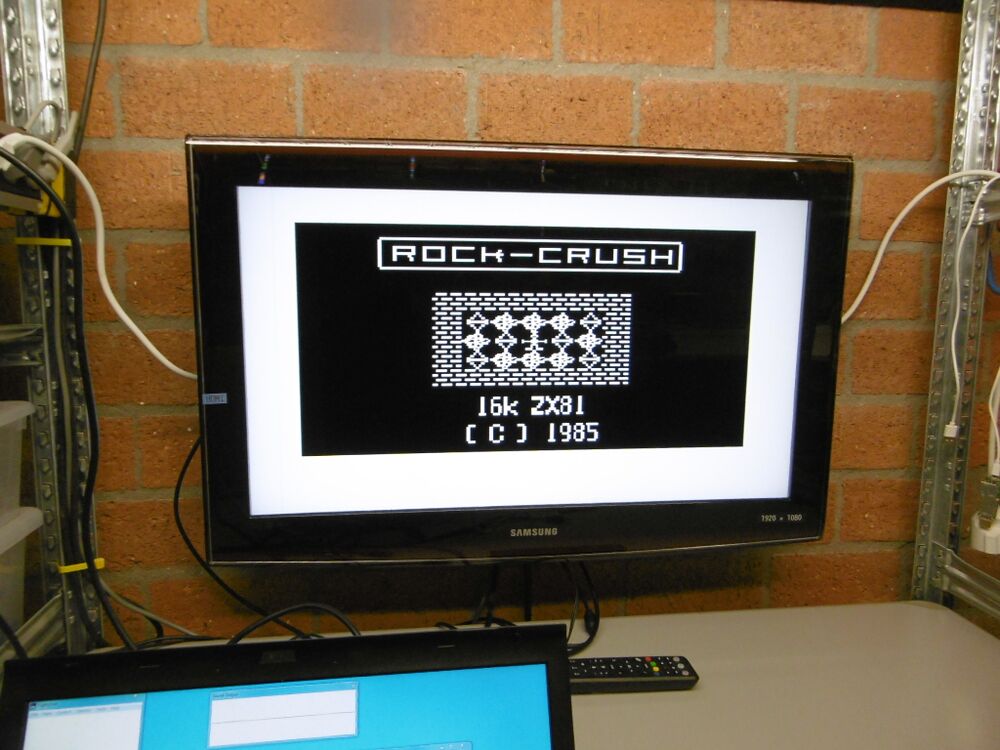
:-( eventually I got eighty-one working, and I figured out how to play a file, a bit of a non-intuitive process. Finally I knew how it worked and I got something that loaded: | |||
[[File:Rock-Crush.JPG|1000px]] | |||
I noticed that indeed I did not get loading bars when loading, only a black screen, but that what what I expected. and so I tried what happened when I did not use load "" just use the blank page with inverted K. I saw loading bars, but only thine ones, and I had to turn the volume to max for that. It seems that the audio level of my laptop with this program is not enough. | |||
Still I managed to load | |||
== Friday 2 December 2022, I ordered ten revision 1.9 PCB's of the ZX81+38, plus ten keyboard PCB's, and five TZXDuino pico PCB's from PCBWay == | |||
I got notice they are on the way to me as I write this text. They will be used to get one Revision 1.9 ZX81+38 for myself to test, and show the keyboard, also to show how a kit would be like. | |||
== Monday december 12, 2022 received the PCB's == | |||
PCB's were delivered today in a small cardboard box, not suitable to be delivered through the mailbox as the box was too large to fit through a mailbox. Also even though it took 5 days to get through dutch customs which I thought was also because I might have to pay taxes that wasn't the case. I did not have to play the deliveryman any taxes due. | |||
All three PCB's were in the box, that is ten ZX81+38 PCB's and ten keyboard PCB's, and 5 TZXDuino-Pico PCB's. | |||
In the meantime a YouTube maker created two vlogs about my ZX-81 clone, ( https://www.youtube.com/watch?v=b6BjFEuRM7A ) and it was all good, although he did not seem to realise that there is a keyboard overlay for my keyboard, he used the keyboard bare, only guided by the texts printed under each button. So I went to my GitHub Page, and discovered the keyboard overlay was only published on the older ZX81+35 page, so that explains it. So I quickly copied the overlay to my ZX81+38 page, and renamed it from ZX81+35 keyboard overlay to ZX81+38 overlay. I also had e-mail from another ZX81+38 fan, and he told me that cassette loading worked fine, but needed a stereo cable, which is explainable as he was using a revision 1.8 PCB, where mistakenly the RING, not the TIP connection was used for audio. Revision 1.9 will work as intended, also with a mono cable, using the TIP (LEFT, or mono) signal. He also gave a link to a LEGO build site where he published a ZX-81 case made from lEGO parts. https://rebrickable.com/mocs/MOC-129979/akilling/lego-case-for-zx81-plus-38/#details | |||
== Tuesday 27, December 2022 == | |||
Forgot to tell that the TZXDuino Pico is working well, I only had to patch the design a bit so that it would become possible to insert an SD-card into the SD-Card reader socket. That is because I hadn't notice that the card has to be inserted on the side with the solder connector, instead of the 180 degrees opposite side. but because the PCB has resistors, and a button on that side. I had to lift up the card holder a bit, and remove one button that was in the way from the board. I did this by sticking a piece of cardboard with dual sided sticky tape under the card reader, and bending its pins down before soldering them to the PCB. I used strips cut from a DIP socket, instead of higher female header connectors to the Arduino sits closer to the board, to reduce height. This way I managed to mount the TZXDuino pico inside a sinclair spectrum 48K. I used two push buttons mounted in the back of the Spectrum, one for "next" and one for "play". | |||
now I know it works, the next time I don't need a socket, and will solder the Arduino nano directly to the board. | |||
I'm planning to repair the problem, by rotating the SD-Card socket 180 degrees. I also will convert the 1206 size resistors to the more common, but still easy to solder 0805 Size. I will upload this version also on GitHub. | |||
== 22, march 2023 picture of my keyboard solution == | |||
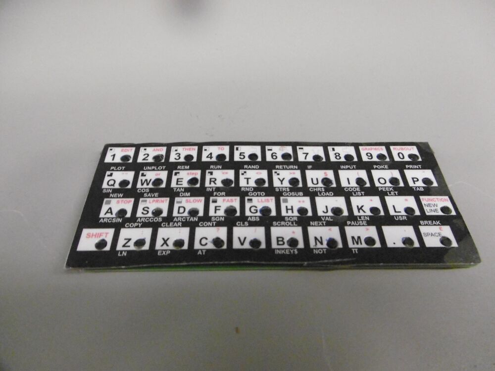
This is the new keyboard PCB with an old crumpled overlay. The overlay isn't cut to size correctly, and the lamination is ugly. | |||
[[File:ZX81+38keyboard .JPG|1000px]] | |||
However the PCB does fit into the ZX-81, it would be better to just mount a new overlay on top of the buttons, and don't laminate the overlay, instead just spray plastic spray over it. | |||
[[File:Keyboard on new PCB mounted on ZX-81.jpeg|1000px]] | |||
from the front you can see the keyboard is quite low (5mm or so), in this example the overlay is quite thick. A thin plasticised overlay without holes would probably be better. | |||
[[File:Keyboard fits on ZX-81 seen from front cropped.jpg|1000px]] | |||
== 28 may, 2023 Tried keyboard again without holes == | |||
I tried it again, with just paper without holes. I plasticized the paper with a spray can. | |||
what I should have done instead was laminating it with transparent foil instead. That would make it more sturdy. | |||
When I stuck two strips of dual sided carpet adhesive tape (double-sided adhesive) the result was that the paper tore a bit, but I ignored it. | |||
I tried to stick it to the keyboard but soon noticed that the paper bent at the edges, I needed a (sticky) ridge around the keyboard, so I used 1mm thick dual sided tape, and this was the result, I also changed the LED for a real SMD LED as I noticed the original LED stuck out too high: | |||
so this was the resulting ridge: | |||
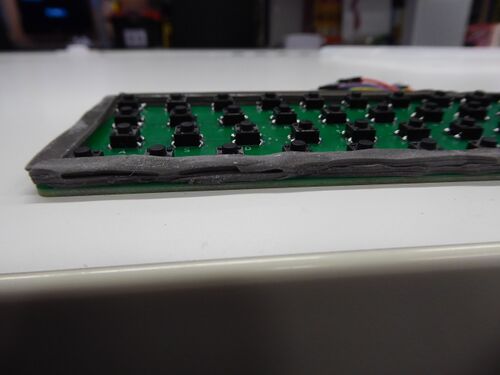
[[File:Sticky Ridge around keyboard .JPG|500px]][[File:Consists of three layers dual sided tape.JPG|500px]] | |||
I used three layers on the three sides, left right and bottom, and two on the top side where the PCB was not flat because of the dupont cables soldered there. | |||
Unfortunately not having laminated the top made the paper a bit wobbly. | |||
[[File:Its a bit wobbly.JPG|800px]] | |||
And the height above the plastic enclosure was about the same as in the past. | |||
Iḿ sure that if I had laminated the plastic on top it would have been a much smoother top, and you still would be able to easily type. | |||
[[File:Keyboard on top of case.JPG|800px]] | |||
== I also tested the joystick == | |||
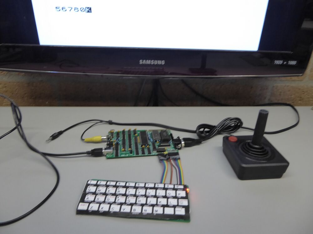
I soldered the DE9 connector for a Atari style joystick and connected a real Atari joystick I borrowed. | |||
I pushed the joystick left down up right and pushed the fire button, and the result was the same as if I had used the keyboard, and had pushed the corresponding buttons, that is the 5, 6, 7, 8 and 0 buttons. | |||
it I heard it works fine with games that use the arrow keys, see this picture: | |||
[[File:Joystick works.JPG|1000px]] | |||
Now I had to make an opening in the right hand side of the enclosure, with a jigsaw that was no problem, | |||
== moved a few screw-holes, for rev 1.10 == | |||
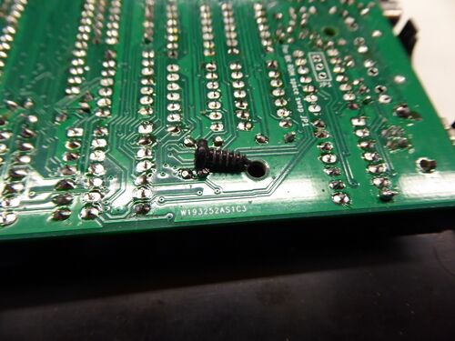
but when I tried to close up the case a problem appeared that I had not seen before, it is not possible to screw the PCB to the case the case, as there is still one hole that is in the wrong location! Its the hole that is close to the text ZX81+38. It is not above the plastic pillar you need to screw into. There are just two screws for holding the PCB in place an this is one of then. | |||
Its this one: | |||
[[File:Screw problem.JPG|500px]] | |||
This is a nasty problem, as it means the layout must change! | |||
Its not possible to simply drill the hole out as there are traces around it, so this will finally become revision 1.10 | |||
note that if you create your own enclosure this is not a problem for you as you can simply modify your case. | |||
I have uploaded the new rev 1.10 version to GitHub, it also includes a new BOM, where one resistor pack has changed from Farnell. As the old version was 4K7 and the corrected one is 10K. | |||
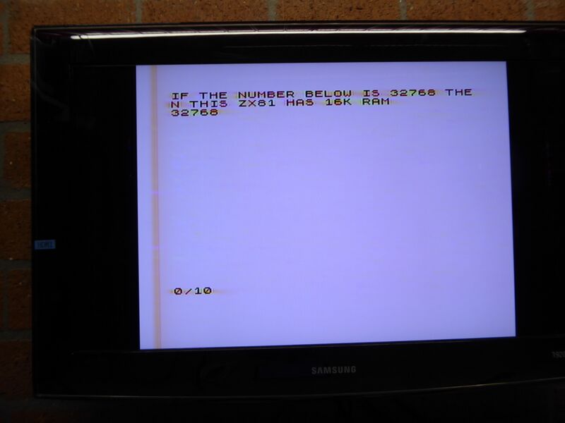
== did a small test to see if my ZX-81 has 16K of RAM == | |||
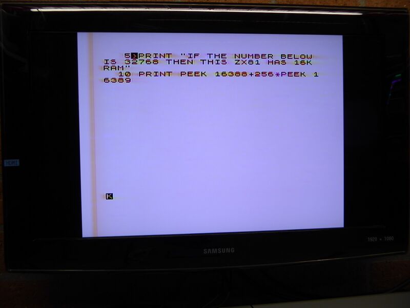
found a small test that will tell if your ZX-81 (clone0 has 16 K of ram, here is the entered program | |||
[[File:Program.JPG|800px]][[File:Result.JPG|800px]] | |||
and here is the result, so yes 16K is acknowledged. | |||
== I have designed my own mechanical keyboard for the ZX81+38 == | |||
Although there are already several full size mechanical keyboards, I decided I wanted to do my own one, one that would perfectly fit the ZX81+38, manly the place of the keyboard connector so it is in-line with the keyboard connector on the ZX81+38 when you allign the left side of the keyboard with the left side of the main PCB (because all the connectors are located on the left side) | |||
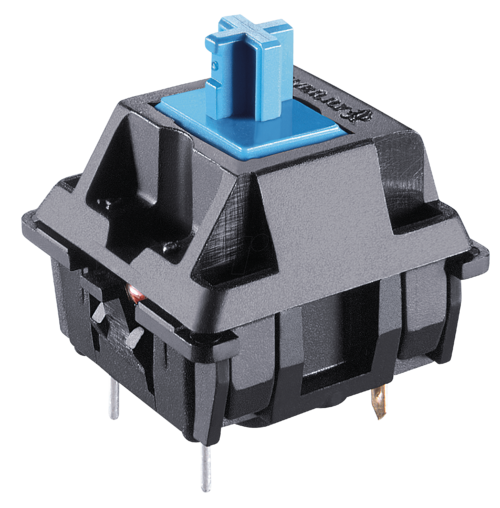
I decided to use the best keys that have a good clicky feel, while being reasonably priced and have a large set of keys to choose from, so I chose the "blue model" the SHERRY KEY MX1A-E1NW standard force, click tactile, PCB Mount, so this keyboard does not need a metal brackets to hold the keys, the keys have plastic pins so they are easily mounted into my keyboard PCB. which also will feature a power LED. | |||
its this key: | |||
[[File:CHERRY MX1A-E1NN 01.png|500px]] | |||
here is the schematic: [[File:Sherry MX1A-E1NW keyboard.pdf]] | |||
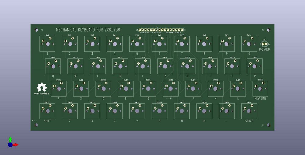
and here is a 3D preview of the PCB, you might think that the buttons are a bit far apart but that is because the keycaps are larger than the buttons. | |||
[[File:Sherry MX1A-E1NW keyboard preview.jpg|1000px]] | |||
I have created a new GitHub repository, and Uploaded the necessary files there: https://github.com/mahjongg2/Mechanical-keyboard-for-ZX81plus38 | |||
== Someone requested a TS1000 version == | |||
The only PCB change is the location of the RCA connector (output of the RF modulator), I considered it and it seems not much effort is required. | |||
This version will be called TS1000plus41, for obvious reasons, and will be a new github project, it will be derived from ZX81+38 revision 1.10. | |||
I will swap the location of the connector, and the clock oscillator. | |||
== TS1000plus41 is finished == | |||
And uploaded to my github page, including the full set of KiCAD files, the schematic, a BOM and obviously the production files, the gerber and drill files in a .ZIP file. | |||
a component placement drawing will be placed soon. | |||
== Uploaded the mechanical keyboard PCB to Github == | |||
Even though I have not yet built one myself I have enough confidence it will work that I decoded no longer to wait, and to release it on GitHub, here: | |||
https://github.com/mahjongg2/Mechanical-keyboard-for-ZX81plus38 | |||
== Got a free ZON-80 clone board for regular ZX-81's from a fan, it works on my ZX81+38 too == | |||
For my ZX81+35 (a previous ZX-81 clone I designed using surface mount components) I had also designed a programmable sound generator, that was software compatible with the contemporary ZON-80 PSG board. You can find it on my GitHub page as "ZON-compatible-PSG-with-SD-interface-for-ZX81plus35-ZX81" . | |||
A certain Thomas Schilling built it, and found out how to get the biting SD-Card interface I had designed using the signal GPIO port of the AY-3-8912 PSG working. I had given up on getting it to work when I found out that the GPIO could not be programmed to set individual bits of the 8-bit GPIO port to inputs our outputs individually, but only as all bit as output, or all bits as input. | |||
I wrote about this project here±: https://revspace.nl/Zon_ZX-81_Programmable_Sound_Generator_expansion_for_ZX81PLUS35_with_working_SD-Card | |||
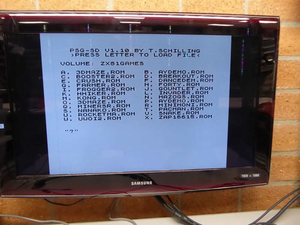
so thomas had built my PSG board for his ZX81+35, and he did find a way to make the biting interface work by inverting the chip select signal (and using a level converter for the data bit), and he wrote the bit banging code to access an sd-card formatted with a FAT filing system. He also wrote a menu driven program to download files from the sd-card. | |||
After he created a working system he let me know he did that, and I patched up my own Zon_ZX-81_Programmable_Sound_Generator_expansion_for_ZX81PLUS35 with the patched Thomas explained to me, and burned his firmware together with the normal 8-K ZX-81 BASIC in a 16K ROM, and indeed it worked, as you can read in the project description. | |||
quite recently Thomas sent me a new version not for the ZX81+35 but for a normal ZX-81, complete with an 8K extension ROM with his firmware, and with 16K RAM. Now I do have a real ZX-81 but unfortunately I do not have a power supply with it, and it has a broken keyboard cable, so I could not immediately test his PSG board, that came fitted into a standard commercial plastic case, only slightly modified, with a large hole for a female edge connector, a hole for a reset button, a hole for the SD-Card, and a hole for an 3.5mm stereo jack. internally his PCB also had an edge connector, but the case had no hole for it. and the way the female edge connector was soldered straight up from the PCB, just like for example the 16K memory expansion, this (male) edge extension connector would stick out on rop, it is unlikely many people would use it, the only potential use for it I can think off is for the ZX-81 printer. | |||
anyhow I decided to try if it would work with my ZX81+38, and spoiler, it did! | |||
I had to do a few things to get it to work, first per default the ZX81+38 has 16K ROM space, not just 8K, as I planned to have the SD-Card firmware in the same physical 16K EEPROM, so without changing the ROM space to 8K there would be a bus clash with hit 8K expansion ROM, and my 16K ROM, so I first changed the ROM space size to 8K by scratching the wire of JP1 (beneath U25) and soldered a wire to the other position. | |||
I tried if I could activate the firmware using calling rom location with the decimal address 12345, with the USR call | |||
LET L = USR 12345 | |||
but the result was not the expected menu, but a crash to a fully black screen. | |||
disappointing! So after some thought about it I removed the RAM chip from my ZX81+38, and lo and behold, it worked!, this was the result! | |||
[[File:P1050837.JPG|1000px]] | |||
It worked, and thomas has updated his menu, as it now has 24 in stead of the older 16 choices. | |||
So I tried a few games, and started with miner5r which worked, but I had no idea how it worked, so I tried a few other games. Packman worked, see the next two pictures, you can change the controls with packman out of three choices, but with the controls set to "cursor" you should be able to use the joystick interface of the ZX81+38 unfortunately I had no joystick at hand, and with the keyboard it is difficult to play, but the game looks very good, and loaded in a few seconds. | |||
[[File:P1050843.JPG|1000px]] | |||
[[File:P1050844.JPG|1000px]] | |||
I have not yet tried the PSG sound, but according to thomas it sounds very good with software like dancing demon, and other temporary ZON-80 compatible software. | |||
Obviously I'm going to create my own version, read this spot | |||
oh, and here is a picture of the zx81+38 board that has the ZON-X80 PSG board for original ZX-81 and ZX81+38. | |||
[[File:PCB Preview ZX81+38 rev 1,10 top now with PSG expansion board.JPG|1000px]] | |||
I changed the project status back to in-progress, and will continue reporting about this expansion board. | |||
Latest revision as of 16:31, 29 November 2023
| Project ZX81plus38 | |
|---|---|
| |
| Most people I showed my ZX-81 clone (ZX81+35) said they liked it, but with such a tiny board and with so many "difficult" surface mount components, they doubted whether they would be able to build this kit, so I restarted my effort, to try to build a 100% compatible ZX-81 clone that anybody could build, but now with commonly available pin-through-hole parts. | |
| Status | In progress |
| Contact | mahjongg |
| Last Update | 2023-11-29 |
September 18, 2019 I started the design
For now I will call it ZX81+38, but I doubt it will be finished in 2019, so it will probably be renamed to ZX81plus39... :-)
P.S. No I won't!
I started analyzing my current schematic, to see whether it contains components that are not available in PTH, and unfortunately there are some, for example "unbuffered inverters" (74HCU04) used in the crystal oscillator, are no longer available in DIP. Also some other logic isn't available in DIP, 13MHz crystals are hard to get in PTH versions, and 6.5MHz are not available at all. I decided to switch from 128K flash ROM to 32K OTP ROM's because the latter are available in DIP-28, while for the former I MUST use a PLC-32 socket. Eproms are a few dimes more expensive there days than OTP's, but DIP sockets are much cheaper than PLCC PTH sockets, and OTP and RAM in DIP-28 placed next to each other are much easier to layout. I also found cheap 32K x 8 static RAMs, also in DIP-28, which will be easier to layout for.
I will design it with KiCad unlike the older version which was designed using Ulticap and Ultiboard.
September 20, 2019 made a preliminary component placement of connectors and drill holes
Measured up a real ZX-81 PCB, and determined the size of its PCB, the locations of its mounting holes, and various connectors, I noticed that the Z80, and its ROM and RAM needed to be in a particular orientation, because of the mounting holes. determined the positions of the Video out connector (although the standard RCA output plug sits lower to the PCB than the RF-modulator output), and determined where the 3.5mm jacks for EAR and MIC should be located. For DC input I did not use another 3.5mm jack, nor did I choose a barrel jack, instead I used a model B (square) USB connector, so you can power the ZX81+38 with an USB charger and a type-A to Type-B (Device) USB cable.
I also placed the expansion port connector, which has the normal contact fingers, but can be enhanced with (gold plated) an angled dual row pinheader connector, so you can choose compatibility, or a more stable connection. I will route to the edge connector, and will place the edge connector "fingers" manually from there.
September 24, 2019 I placed most of the components in the schematic
I was curious if my USB replacement logic would fit, so I quickly placed most of the needed logic in the schematic, and annotated them the same as my SMT version (logic simplification and renumbering will come later), and gave them PTH footprints. At the end of the evening I had enough of the schematic elements to do a forward annotate, so I could do an estimate of it would fit, the result is visible in the top right hand corner of this page. To my relief I found that it should fit (its just a rough estimate obviously).
September 29, 2019 continued with component selection and routing of the schematic
I found out which combination of gates and such resulted in the fewest physical IC's, swapping some gates around, and trying to find replacements for single gate IC's, which do not exist in DIL. changed the AND that combined HSYNC and VSYNC to and EXOR as during VSYNC HSYNC pulses actually appear as inverted in the VSYNC signal, but perhaps I should check my logic here carefully.
I also changed the AND combining video with the nPORCH into a NOR, with inverted inputs, also something to check later.
I had forgotten how much trouble it is to get the connections of the Z80 databus to the NOP enforcer, and pullup resistor pack right, probably I will need lost more wire swapping action to get a somewhat easy to route solution.Laying out this board will be an interactive and iterative process, with lots of forward annotations, and corrections in how everything is connected. I won´t swap data and address lines around for the EPROM (or we have to do some swapping of the EPROM content too, and that is not what I want). This implies that RAM lines swapping won´t happen either, as the ROM and RAM wiring is almost identical.
October 1, 2019 continued
Stupidly I lost previously placed mounting holes, that took hard work to do , because I imported a schematic that didn't have them, so the forward annotate function removed them from the board. I noticed they were gone when I looked at the preview picture. So after uttering a few choice words I have now entered mounting holes in the schematic, and once again started with their placement. Luckily I had made a 1:1 (real size) printout of the PCB WITH the locations of the mounting holes, which makes measuring up their locations a tiny bit easier. Now I also differentiated between 3.0mm holes for the screws that close up the case, and slightly smaller (2.5mm) holes for mounting the PCB to the enclosure. I also re-read some old correspondence about using an EXOR for combining HSync and Vsync, and saw that there are technical reasons why using an simple OR function will be better, So I will do that instead. I also realized that from revision 2.2 to the current revision 4.0 of my ZX81+35 the sync generation logic has had a big overhaul, that has never been tested. Also I was warned that my component placement drawing of ZX91+35 contains an error, listing U13, as a 74HC32, (OR gates) instead of a 74HC00 (NAND gates). I wanted to check if the BOM had the same error and tried to download it from GitHub, but for some reason I only got a .ZIP containing gibberish instead of the spreadsheet. Both problems I will fix soon. Also the person who noticed the U13 problem also has problems with horizontal sync not being present, and I have to investigate that too. He promised to send me one of his two build up prototypes that have this problem. on a positive note, he is using my keyboard PCB too, and it is working fine!
October 6, schematic mostly finished
Yesterday I finished placing of the mounting holes in the PCB, today I mostly finished the schematic.
Replaced main picture with the preview schematic as a .PNG picture.
October 9, schematic rev1.0 finished
Schematic finished for rev 1.0, updated schematic File:ZX81plus38.pdf, plus preview schematic pictures. Next up, importing the components in the PCB layout, and placement of the parts. No attempts have been made yet to try to support multiple types of ROM/EPROM/FLASH, like the original ZX81 ROM. But this schematic should be complete. New is my attempt to support the canonical cassette loading video bars.
October 13, 2019, schematic rev1.1 (some errors fixed, added ZX81 ROM support)
Found, and repaired some errors, when doing electrical rule checking, (non connected power supply pins, no footprints assigned, such errors). nNMI is now directly connected to A6, without a resistor in-between. Improved the way cassette input shows up as loading bars by using and AND port. Noticed many labels where the "'" (bis) marker was changed to something very similar, but resulting in no connections between various connections having a "'" (bis) sign in the label, checked all nodes with a bis marker (D0' to D7' and A0' to A8') for connectivity, and repaired the labels with a problem. Also, I corrected some labels where I used the backslash to denote in inverted signal, instead of the lowercase "n" I used everywhere else.
also found a small error in the original ZX81 schematic, which claims that the D7 signal is NOT connected through a 470 Ohms resistor, but actually, it IS! (I measured 470 ohm between pin 13 of the Z80 and pin 1 of side A1 on a real ZX-81), so the "D7" label on the expansion connector should have been written as "D7'".
Added several 3-pin jumpers so that the EEPROM socket can be configured to accept a ROM from a real ZX81, These jumpers are pre-connected, and per default configured for a 27C256 EEPROM, two of the jumpers can also be used to select one of four possible 8K images that can be contained in a 27C256, per default only the first 8K is used. Jumpers will be "virtual", meaning they will probably be mounted on the underside of the PCB under the EEPROM, and to change for a ZX81 ROM you will need to scratch through the pre-connection between pin 1 and 2.
All components are now cleanly forward annotated, so next job will be component placement.
Schematic is now revision 1.1 File:ZX81plus38 rev 1.1.pdf
October 15, 2019, finished schematic rev1.2 (functionally complete)
Added support for loading bars, using spare gates, only new part is one pull-down resistor. added some explanatory texts, changed U22 so that its wiring is optimal for keyboard column readout placement. converted the logic type to active low logic symbols where that was more logical, so its easier to follow the logic.
This schematic should be functionally complete, (if nothing unexpected happens) changes beyond rev 1.2 should only consist of pin or component swapping optimizations, and component renumbering (after I did the placement).
Revision 1.2: File:ZX81plus38 rev1.2.pdf
October 20, 2016 rev 1.3 supports 16K ROM's
I realized that some people might want to extend the Sinclair BASIC ROM, or replace it with something else, and might need a larger ROM, so I added a (virtual) jumper to enable 16K ROM's to the ROM encoder and added A13 to the EEPROM address lines. revision 1.3 with 16K ROM support: File:ZX81plus38 rev1.3.pdf
October 30, 2016 First component placement
I managed to place all the components on the available IC's,but barely so.
I will probably need to do a lot of optimization (IC and gate swapping) to minimize as much as possible the routing needed, as there is almost no space left for routing.
November 6, 2016 re-shaped the DIP pads to accommodate routing two wires between pads
As you can see in this picture, on various places it becomes impossible to do horizontal routing of connections, if you can only route one trace between two pads.
You can also see I modified the PADs to make this possible, I decided to use a PAD height of 60 mil (with a hole size of 35mil, and a pad width of 90mil), so there is 40 mil between two pads, for two traces you need two traces of at least 0.15mm inter-spaced with three spaces of also at least 0.15mm. So 40 divided by 5 = 8mil, or 0.2032mm. I decided to use 0.2mm traces .
Next job is to simplify the rats nest by swapping ports (and or components).
November 13, 2019 Did a lot of placement optimization
Now the schematic is updated to revision 1.4. File:ZX81plus38rev 1.4.pdf due to swapped ports.
Not only a lot of ports have been swapped, but also the component placement itself has been modified a lot.
This is revision 1.4 as a 16 color .PNG (in full resolution), open to see full resolution.
November 20, 2019 finished placement, did some power routing
based on schematic rev 1.4, I further optimized placement and started with power routing (GND and +5V) as the basis. This screenshot shows my progress:
December 10, 2019, partially routed
routing proceeds nicely, this is the current situation a few weeks later:
January 14, 2020, some progress
The easy part is done, routing now becomes more difficult.
January 22, 2020 more progress
January 28, 2020
February 12, 2020
Removed a lot of connections to the expansion connector, as to improve the overview of the connections.
As for now, power and databus connections are present, as well as a few address lines. When the currently active connections are done, I will start adding address lines, and the most important control signals, then attempt to add the rest of the connections.
February 19, 2020
Finished routing! Also Added enough connections to the expansion port so that I/O based expansions boards should still work (printer, Programmable sound generator board, joysticks etc). Memory expansion is not really useful, nor DMA. so it is not supported. in practice this should not be a problem.
After I finish extensive cleanup I will add copper fill (GND).
February 26, 2020
I decided to do an ultimate attempt to route the missing signals to the expansion connector, so that I could also support external memory, and I succeeded in routing almost all connections, just two signals /BUSACK and /WAIT are not connected, but I'm planning to attempt these next week. :-)
March 4, 2020 layout finished
Finished /BUSACK and /WAIT, did DRC checks, added copper fills. created gerber files to do a productivity check.
I uploaded the file to a PCB producer to check it for aberrations (violations of their production rules) and I'm happy to say there were none. This is how the top layer (without solder mask) would look like:
and this is the bottom layer:
I still have to work on the solder mask, (especially removing solder mask on the edge connector) and on the silk screen (paint)in the form of texts and logo's.
Extra vias between top and bottom copperfill should be added wherever possible, and where possible ground traces should be added between two copperfills tightening the ground plane.
March 11, 2020 Added soldermask, and silkscreen
I added a soldermask, which wasn't present last week. Made openings in soldermask for edge connector, and crystal. Added silk screen text, component values etc. Enhanced ground plane with via's, and fortified +5V traces with copper planes.
This is how the PCB will look, top view:
and bottom view
March 16, RefSpace is closed!
Still to do (when Revspace opens again): clean up pre-wired jumpers, move all of them to the bottom (as they will be underneath components when they are on top). Add the default RAM size jumper for JP12 and set it to 16K (To GND, the most standard setting) 32K is nice but non standard. Also move bottom silk screen markers to correct positions. label all jumper positions as a table on the bottom silk screen (explain their functions). Also add rectangular boxes (silk screen) around jumpers.
The jumpers are:
JP1, select ROM size, default = 8K alternative = 16K
JP4, place to select 50Hz, open = 60Hz
JP5, Invert video, default = black text alternative = white text
JP6, first pixel fill, default = white, alternative = black
JP8, U5 pin 23, default = A11, alternative = A12
JP9, U5 pin 26, default = A13, alternative = +5V
JP10, U5 pin 20, default = nROMCS, alternative = A11
JP12, U3 PIN 1, default= GND (16K), alternative A14 (32K)
April 10, ZX-81plus38 PCB is finished
working from home, because of the corona crisis I finished the PCB layout. Made all pre-wired jumper connections accessible from the back side, and placed some descriptive text on the back about what these jumpers do. Also added a default wire for 16K/32K RAM with the default of 16K, for best compatibility with the original with a 16K memory pack. Don't forget to place the two jumpers for inverse video mode, and place default jumpers on them, in the position that pleases you, but don't forget that the real ZX-81 displayed black text on a white background. One jumper inverts the bits, another determines the "fill in color", with this setting wrong white or black stripes can appear between the letters. JP4 is normally left open, unless you are using an NTSC TV instead of the normal PAL TV. JP1 only has to change if you use a larger (than 8K) (E)PROM or OTP-ROM. When using a Atmel AT27C256R (32K) the code fits four times in the available size, I would recommend programming four identical 8K copies in the ROM.
This is a picture of the final PCB: Top:
and bottom:
I also made a component overview drawing
I'm working on a bill of materials, and a final schematic (black and white .PDF) Currently I have uploaded a .ZIP with gerber and drill files to github, here: [1]
my GitHub page is here: [2]
Its a bit hidden in the LICENSE.md directory, that will be corrected, and other stuff will be added, such as the BOM and KiCad files.
by the way, the PCB is 142.2mm wide en 99.0mm high, you might need those dimensions when ordering a PCB.
Due to the COVID-19 crisis progress has temporarily halted
RevSpace was/is in lockdown, and working on this project from home proved problematic, but slowly I will pick up the work again. next will be the Schematic in black and white, the BOM, and a keyboard layout specific for the ZX81plus38. Hopefully I didn't do the previous keyboard with the older windows CAD software, as if I did I have to do it over with KiCad.
I managed to work from home
I finished the promised schematic in black and white, also found and corrected a few minor mistakes, 620 Ohm resistors do not exist in the E12 range and should be 680 Ohm, and RP2 was named incorrectly. this is the final schematic of 12 September 2020: File:ZX81plus38Rev1.4BW.pdf
I also finished the BOM of the ZX81+38, so now you can order the components. I used two sources for components, as neither of the to had all the components that are necessary. I used farnell and mouser as suppliers, and between them they had everything that is necessary to build this ZX-81 clone. This is the spreadsheet in open office (.ODS) format. File:ZX81plus38 BOM.ods.
I will try to upload these two files to github too.
Revision 1.5 with various corrections should now be working
In this schematic all the reported faults and requested improvements are implemented. File:ZX81plus38rev1,5.pdf
The following changes were made:
- C1 and C2 of the crystal oscillator were lowered to 4.7pF
- the signal n6.5M was removed, and flip/flop U18B was clocked with the non inverted clock 6.5M
- the removed inverter U21D was used to build a new WAIT generator circuit in place of U18A, together with OR port U12B. the previous version did not work mainly because of the flip/flop not working as a WAIT generator. To be able to externally for the /WAIT signal low a resistor R20 was placed in series with the nWAIT output.
- The RCA PSG01546 plug had a wrong footprint, and so could only be place 180 degrees rotated (not that it would work if you did). I found a replacement RCA plug that could be inserted, the CLIFF FC68391, and updated the footprint for a perfect fit
- on the expansion connector I had swapped A13 and A14, so I corrected it
- also on the expansion connector JB1 pin 2 was tied to +5V, but this pin was meant for +9V, so I put a jumper between +5V and this pin, so the pin can be jumpered to +5V or tied to an external +9V source
- The ROM socket was designed for an OTP (one time programmable, an EEPROM without its glass erase window) and with wire links on the bottom you could (re-jumper) by scratching a track and wiring between the other pads the socket for the original ZX-81 ROM.
Some users asked if I could also support EEEPROMS, and although this was already possible pin 1 (A14 on an EEEPROM) was tied permanently high, so I made it that you could disconnect Pin 1, and tie it to something else, like a switch.
- i had created the option to invert the video with two jumpers JP5 and JP6, but got the complaint that if you forgot to place these two jumpers you would get no video, so I also pre-connected these two jumpers for default white screen with black letters.
Its still possible to get a black screen with white letters, but you have to scratch through the default pre-connects, and add a wire link
- I got asked why the keyboard wires were not simply one strip of holes with a 2.54mm pitch,but was deliberate, the previous version has three extra holes for a power LED, and a reset button, ad I had removed these. So I added three holes, and put all holes in the same raster. Its possible to have a power LED on the keyboard now.
- I enlarged the mounting hole bottom left, above the text "ZX81+38"two as requested.
- Jumper JP1 was wired "in reverse", but as A13 was correctly connected to pin-1 of U23A that wasn't a problem
If you have a revision 1.4 PCB, you can get it working by doing three things:
- Use OTP's, not EEEPROMS (which are six times more expensive anyway) and fill the 32K rom with four copies of the ZX-81 BASIC.
- Remove the output of the flip flop U28A, so that /WAIT is not driven,
- and replace the WAIT circuit with either the two transistor improved wait circuit from wilf ritger, or the wait circuit of revision 1.5 with an inverter and OR port
- disconnect U18B pin 11 (clk) from the inverted 6.5MHz clock, and tie it to the non inverted 6.5MHz clock, closest point to connect to is pin 2 of the shift register 74LS165 (U9).
Now the clone should work.
Layout ZX81+38 rev 1,5 finished and checked
This is the new layout of revision 1.5, it has been checked for DRC errors, and this is a screenshot of how the PCB will look like true size is 142mm wide and 100mm deep, so this picture is nearly true size (depending on your monitor): Top
and bottom:
A few found error makes Revision 1,6 necessary
We (the members of the microcontroller.net forum) have found another small error. The keyboard matrix uses address line A8 to A15, but A8 of this range of signals goes through a 1K resistor (signal is called A8' ) this is undesirable! Just as A9 to A15 do not go through a 1K resistor so shouldn't A8 go through a resistor, as otherwise the data-line driven by A8 cannot pull the signal to nearly ground level. and if a user presses two keys at the same time A8' can go to a wrong signal levelaffecting what the CPU reads from ROM or RAM resulting in a crash. So the layout must be changed so that A8' becomes just A8.
Now started at this change which will become revision 1,6.
this is the schematic, with a tiny change: File:ZX81plus38rev1,6.pdf
The layout change was far more challenging, as I had to route a new signal (A8) throughout the PCB, from R1 to D6.
Actually I was wrong, and the new routing wasn't actually needed, it was just that the pullups of 4K7 are just a bit too strong, and should have been 10K, with 4K7 the resistor divider created by the 1K address-series resistor, and 4K7 pullup made it that the logic level on the keyboard data line of a pressed key would not go low enough, and if you pressed a second key an illegal logic level could exist on A8' with 10K pullups this would be much less likely. Still, there is no reason to return to the old layout with A8' connected to D6, the original ZX-81 did that too (easier to layout I presume) so Ill keep this layout, only changed the schematics to a resistor array of 6 x 10K instead of 6 x 4K7. I kept the version number the same (rev 1,6)
This is the new TOP side of rev 1,6
and this is the bottom side:
11 november 2020, I received a rev 1.6 PCB, and parts
I'm now in possession of a rev 1.6 PCB, and all the parts, including a programmed (OTP) ROM, thanks to donations from persons building my ZX-81+38. Unfortunately due the revspace being in complete lockdown, I cannot build up my copy of the ZX-81+38, nor can I check if the PCB fits into the regular ZX-81 enclosure. so until revspace re-opens, (enough so that I can go there and lend a soldering iron, and check if the PCB fits) Im not able to continue building and testing the ZX-81 until say half december.
Perhaps one thing I can do is designing a ZON clone board for the ZX-81+38, as I have done for the ZX-81+35.
26 november 2020, I found a suitable soldering iron at home
I was looking for a red pencil iron I thought I had, but I cannot find it, instead I found a cheap 15Watt iron still in its blister package, I did not know I had (no idea where I got it from), but its useable and suitable for 240V (its not a 110V iron, from the CRT repair workshop I did). I also found a solder iron holder with a sponge into which this solder iron fits nicely, and a roll of suitable (60/40 solder with resin core) solder. And I also found an extension cord so I have more than one mains socket at my kitchen table. So I'm all set to start with the revision 1.6 PCB.
I'm slowly recovering from my "covid recovery syndrome" sickness (which felt like a very bad worsening of my asthma) i'm slowly getting a bit more energy, in the past 5 or so weeks I could not even walk 100 meter without "blacking out" and having to sit down. Which made shopping for food very difficult, even though I practically live above the supermarket. Hopefully I will get back my energy, so I can start soldering.
P.S. I went to a cardiologist to have my heart checked out, but there doesn't seem to be any problem with my heart, and the visit only resulted in a small change in my medication, and obviously in a big relief. Very soon I will be vaccinated for covid. Hopefully this will give me a bit more energy as my energy level has been very low the last half year or so. I have not done much work on my own prototype (revision 1.6 board) I just soldered about 3/4 of the sockets. Hopefully I will do some more soon. I'm curious if it works exactly as I expect it, especially if the loading bar emulation logic works exactly as I planned. Several builder have announced that the revision 1.6 now works "perfectly" (for them). I also need to get my earlier keyboard PCB, which I suspect is still at Revspace. The expectation is that many covid limitations will be lifted in a few weeks.
by the way, you can find all files you need to build my clone at https://github.com/mahjongg2/ZX81plus38
If you want to communicate with me you can post in the ZX81plus38 thread I have on the raspberry PI forum here: https://www.raspberrypi.org/forums/viewtopic.php?f=62&t=254492 if it is locked for new posts (it will automatically be locked after 180 days of inactivity) click on the flag icon above the post to flag a moderator, and ask to unlock the thread.
April 17, 2022 I Produced a component placement diagram for rev 1.6
To assist building up my own prototype board, I have drawn a component placement diagram, while editing it I discovered how much this version has changed in regards to the version I used as a basis, (I think it was revision 1.4) but AFAIK this diagram is now correct for a revision 1.6 board. I will soon used it, and hopefully, if there are any problems with it I will catch and repair the errors. While doing this I also discovered a few small corrections in the Bill of material (BOM) file, and corrected those too. In the schematic a few resistors were listed as 640 Ohm, that is incorrect they should have been 680 Ohm, 640 ohm isn't a standard value, also an extra 680 ohm was inserted in the nWAIT signal.
here is the drawing:
I finished soldering all the sockets and parts on my copy of the ZX81+38! I also tried powering up the board (without any IC's placed) and measured if all IC's received power, and if the polarity was OK, it was, and there were no shorts either. Here is a picture of the result. I have to place all IC's (I should have them), and program the EPROM (27C256R-45PU) using the REVSpace TL866II plus XGecu programmer, meaning I have to install the programmer software on my laptop.
Here is a picture of the built up ZX81+38 PCB:
I also made a drawing explaining the thee choices of ROM's that can be used for the ZX81+38
- An original ZX-81 ROM
- an 32K OTP (27C256) used as a 16K x 8 ROM, with the option to put Thomas PSG-SD card reader software in the second 8K of ROM, the default option
- a 32K EEPROM (28C256) also used as a 16K x 8 ROM, same as the OTP, but useful if you expect you will need to reprogram the ROM often
reference the schematic (revision 1.6) if you want to change the wiring for either the original ZX-81 ROM, or for the reprogrammable EEPROM, for the default use of an OTP 27C256 no changes to the wiring are needed, not that changing the wiring involved cutting traces between "jumper locations" on the back of the board, and wiring the other configuration with this wires, obviously you can't install real jumpers as they would interfere with the ROM socket. Cutting and wiring is only needed for something other than the 27C256 OTP ROM!
Note that there exists a 27Cxxx EEPROM that is an EPROM that is electrically erasable, the WINBOND W27C512, which is also twice the size as the normal 27C256, it needs no programming voltage and uses PIN-1 for one more address line (A15) as it is normally tied high it acts like a normal 27C256, except that the ROM content must be programmed in the top half of the memory. Alternatively you could isolate pin 1, and use another switch to switch between the two 256K halves.
Also not that the latest PCB already supports a 16K "rom space" in the memory map, occupying the first 16K of address spacing, all the rest of memory space will select the static RAM, probably partly in two 16K memory mirrors.so the ZX-81 will only see 32K not 48K (with the HM62256BLP 32K SRAM chip used)
May 24, 2020 slowly making progress
I managed to get Windows 7 booting again on my laptop, but its quite a convoluted progress. I have a multi boot menu from my Linux Mint install, but when I chose windows 7 from the boot menu windows claimed "something has changed and I can't boot, please use a windows 7 install disk to fix the error" which I tried, but windows claimed not to be able to use my install disk, so I was stuck! And I still wanted to use the TL866 II plus programmer with windows (under linux there is only a command line driver, which makes using it impossible for me, don't get why there is no GUI for it!). But I found a way to start windows 7, the trick is to press enter to interrupt the standard boot up process of my laptop, then I could press F11 to start in Recovery mode, which again started the same ""something has changed and I can't boot" message but this time when I press ESC in that screen windows boots! So I booted windows, found new software for the (greatly enhanced TL866 II plus) programmer from a chinese site (if you choose the "download from local second download option it downloads an installer packed as an RAR file, so I also had to install WINRAR, and I installed some kind of HEX editor for good measure. So the programmer software was unRARed an installed which went smoothly, and I had working programming software. With that I found out that one of my two 74HC14 IC's was defective (use the 7414 options to test) that was due to me being stupid (foggy in the head) and placing it in it's socket the wrong way around, and no 74HC14 do not tolerate being fed negative 5Volt! but the other 74HC14 was fine. I have thought about why the 13MHz crystal oscillator did not work last time, even with the "good chip", and came to one of a few theories, the first is that the 2M2 feedback resistor was too large (in value), so I replaced it with a 1 Meg resistor, the second problem I could force is that a HC14 hex inverter might not like having its other five inputs floating, so I temporary fixed it so the other 5 inputs were either tied to +5V or another inverter output. next week I will test the oscillator with an oscilloscope, hopefully it will start working. I also was give three 27C512 EPROM's which the programmer said were not empty, but the donor of the chips found out these can actually be reprogrammed! they are in fact EEPROM's, not OTP's. also I was given a 28C256 by a generous german builder of my ZX81+38 (who also donated many chips and a revision 1.6 PCB). I found with the programmer this chip was filed with four copies of the ZX-81 ROM! so I had the code which I could download to my laptop from the EEPROM, and program twice in the 27C512, so it has eight 8K copies, which should work with my Revision 1.6 PCB without any modifications needed. also my 32K RAM chip tested good with the programmer. So now I have three 27C512 EEPROMs with ZX-81 code, and a 28C256, but that one needs patching the board so I probably will not need it, but as a source for ZX-81 BASIC ROM it was great.
next week I will continue with the xtal oscillator. Obviously windows wanted to update first 9 updates, then after a restart (to see if I could re-boot windows without needing the installer CD) it again wanted to install again, next time I will reboot windows it will probably want to finish the install as windows always does, I hate that! It was the main reason to switch to using Linux Mint!
juni 1 2022, crystal oscilator is working!
Found out I had a defective 13 MHz crystal. Tested with a 12MHz crystal and it worked (with 1M feedback resistor, and the original 74HC14). So even with the worst type of inverter (schmitt trigger) it works, but I have tied all other inverter inputs to a stable logic level instead of floating, that initially might have had something to do with it. probably unsoldering the crystal broke it, another potential problem might be that the top of the solder pads short to the metal of the crystal, so I advise to put a piece of paper under the crystal to prevent a short. Will update schematic and BOM with the optimal IC, the "unbuffered" version of the 74HC04, the 74HCU04, which is the fastest inverter , don't understand why I chose the schmitt trigger inverter 74HC14, which is the worst possible choice, as it requires a much larger input swing, and introduces a longer delay! will update Github, also R21 is the series resistor of the power LED, which is only needed when you use a power LED (on your keyboard PCB) I suggest using 220 Ohm.
So now I need to get another 13MHz crystal, and a 74HCU04.
P.S. Mario "kinzi" Kienspergher wrote me that the not working crystal oscillator is almost certainly due to the use of schmitt trigger inverters, and that his experience is that it can work with 12Mhz while not at all working with 13Mhz, Jens hauslage wrote he got the oscillator working by lowering the 2M2 resistor to 1M, and replacing R30 the 1K series resistor with an 68pF capacitor, he now has the inverted K cursor and is working on the keyboard now.
juni 7 2022, still have crystal oscilator problems for my own copy
Update, found out my 13MHz crystal is absolutely defective, tried to use some other inverter IC's but (opviously if you think about it) none of the ones I tried work (74LS04 and 74L04, obviously I need a CMOS inverter), so the problem stays that I need to buy a new 13MHz crystal, and a 74HC04 or 74HCU04 which is difficult for now because I no longer have access to many sources such as Farnell (without working for a company). I will keep trying. found a 13.025 MHz mini crystal I might use.
juni 22 2022, got a free Xtal and 74HCU04, Finished Revision 1.7
will try the new crystal and 74HCU04 next time when I'm at Revspace. I also got An I/O expansion board (8 input and 8 outputs) from the same ZX81+38 enthousiast that gifted the Xtal and 74HCU04. In the meantime I got a few tips and requests from him which led to me creating revision 1.7: The changes (relative to 1.6) are:
- Changed footpad of crystal oscillator to a footpad that supports both PTH and SMT crystals. You do need an isolator between crystal case and pads when using a crystal with leads if you must use it as a pin through hole crystal, to avoid shorts. When using an SMT crystal, it will come with a plastic base, and shorts are not possible simply solder the wires to the pads from the top side.
- Changed R29 to 1M, U21 to 74HCU04, also changed RP2 to 8x22K and changed the series resistor R21 to 330 Ohm (was 100Ohm) all as the latest BOM tells you.
- changed the default JP1 jumping so that there will be 16K of ROM-space, not 8K, if you want to use four separate 8K images then switch JP1 back to 8K ROM-Space. then you can use two switches to drive A13 and A14 with switches, after having disconnected the pre-wired trace between jumpers JP9 and JP10.
- The same user that gifted me stuff also remarked he had to twist the 5-wire data lead (foil) because J3 was reversed in orientation, this must be the last of many keyboard wiring errors I have made, so I need to also create a specific ZX8138 keypad with wiring 100% compatible with a real ZX-81. note that this means the keyboard data lines on the ZX81+35 are inverted too, I will do no changes to ZX81+35 anymore, sorry.
The new schematic as .PDF File:ZX81plus38 Rev 1,7.pdf
and updated placement file
It happened I uploaded all ZX81+38 revision 1.7 files to GitHub
Updated files, are the Production files (.zip) with all the gerber an drill files to create the PCB, a schematic (in monochrome) of revision 1.7, and a picture of the updated placement file. The earlier updated BOM files is compatible with revision 1.7 and now also has more sources listed for components. To top it all of I uploaded the 8K ROM file for a ZX81 (clone) which is legal as the ROM was freed to the public domain. I'm still planning to release the full set of KiCad files (including extra schematic and footprint libraries) to GitHub in the near future.
June 29, 2022 The crystal oscillator is working!
I am using a 74HCU04, but no doubt a 74HC04 will work as well. I now have soldered the crystal directly to the board without sockets, and used a small piece of Kapton tape to isolate the metal body of the crystal from the pads below.
July 6, 2022 I made an observation while building up my copy of the ZX81+38 that shook me
I made a (for me) stunning discovery, as I said earlier I derived the ZX81+38 clone from my fully working ZX81+35 clone, which was built up from SMT (surface mount) IC's and in it I exclusively had used 74HC logic, even for the dual four input NOR gate the 74HC4002 which is actually a CD4000 family chip. And certainly the crystal oscillator should not be the wrong kind of logic, initially it was a single-gate CMOS logic unbuffered inverter the SN74LVC1GU04 why I replaced it with a 74HC14 I will never know. So when I read complaints that I had "mixed up logic families" I was initially unconcerned and thought that maybe I had replaced some 74HC ic's with 74HCT ic's, because a DIP version of some IC's were easier to get in 74HCT logic than in 74HC logic, and in my mind not a single 74LS family chip was used. But that illusion was shattered when I was building up the board using my self made component placement drawing and I saw many IC's being listed as LS logic! That is one reason why you will normally not release a design before you build up and test it successfully, as in that stage you are bound to find silly mistakes like that.
Shock-horror how could this be, and why didn't I noticed this obvious error before, I checked the BOM, and indeed there too I noted that LS logic, not HC logic was often used! Now I have no doubt that HC(T) and LS logic CAN BE MIXED, in a 5V powered design, but as I said I did not deliberately changed any HC logic family IC to an LS IC'!
Somewhere something must have gone wrong for this to have happened!
I assume the fault occurred because I re-drew the schematic in KiCad, for my original (paper) ZX81+35 schematic and I remembered from that conversion project that not all IC's I needed where in the KiCad library in the form of DIP 74HC logic IC's, so sometimes I was forced to use to use the 74LS DIP library, and change the logic type (IC label) to 74HC from the original 74LS logic label, in that process something must have gone wrong! All the places where I deviated from the 74HC family and the labeling was changed back to 74LS that is in error!
As the BOM was derived from the schematic, and the build up diagram was derived from the silk screen diagram and the BOM it contains the same errors.
But again, this doen't mean it won't work, it should work, only drawing a bit more current than it should. As I said before I received news that someone had built u this clone with IC's he had on hand, which where military LS logic (54LS logic) and it worked fine. But this does explain why observant copyists of my design noticed the mix of logic, which I completely failed to detect.
I want my designs to be perfect, so I will correct the schematic, the BOM, and the placement diagram.
Another observation I also made is that sockets with machined (round) sockets are very bad at accepting imperfect IC's, so I sometimes needed half an hour to minutely straighten out IC pins, as the socket otherwise would not accept them. Recently I saw a youtube video where a retro-computer repairman repaired an oddly build up C64 by replacing its mixture of sockets and he remarked that he much rather used dual wipe sockets because machined pin sockets are notoriously bad a making reliable contact when a bit of the pins of a DIP IC was cut off, and that dual-wipe sockets were not like the cheap single wipe sockets, but were in fact even better than machined sockets. So please do yourself a favour and use dual wipe sockets not machined sockets.
July 10, 2022 updated rev 1.7 schematic, Gerber/drill and placement drawing
The new schematic rev 1.8 as a .PDF File:ZX81plus38Rev1,8.pdf
And as .PNG picture:
The new placement file, with only HC logic:
July 13, 2022 tested my copy of the ZX81+38
I had a short time to test my copy of the ZX81+38, short because I had to make sure the TV I used was capable of accepting a composite video signal. To do that I used my smallest NES in a joypad, and I concluded the TV produced (only) a monochrome video picture.
I had little time because I came in late at Revspace, and my first priority was to replace the CR2032 battery in my recently rediscovered Dreamcast, which I didn't knew I still had. But after ten years of inactivity its battery was dead. So I opened it up, and found that the battery was soldered to a PCB, without a battery holder. But I found pieces of metal with which you can create a battery holder, if you solder it to a PCB. After some thought I found a piece of dual sided clad-board, which I could cut to size and solder to the metal, then a few wires could be soldered to both ends of the dual sided board, and I had 3.3Volt between a red and a black wire. I soldered the wires to the removed remains of the battery, and had opened the solder holes. After that I could use some dual sided sticky tape to hold the battery in place. I tested the dreamcast and my replacement battery worked. I realistically had 15 minutes left, so I decided to do a quick test of the ZX81+38, unfortuantely the result was disappointing an all black screen! No video at all!. Its not what I had hoped for, but I don't even know if the EEPROM was programmed, let alone programmed with copies of the ZX81 ROM code, so next week I will start testing what is wrong.
July 14, 2022 Updated the layout with correction of NPTH holes and USB connector positions
With help of a real ZX81 PCB, and the enclosure of a real ZX81 I could check if all the non plated holes (for screws) were in their correct positions. I found that many holes were between 0.5 and 1.5mm from their correct location, and managed with a calliper, and ruler to find aberrations, and correct them. I also moved the USB connector o.7mm toward the audio connectors, so the square type-B USB connector could be inserted while the PCB was mounted in the original case, without having to cut away any plastic from the enclosure. I generated updated gerber files, which I will upload to GitHub after checking them with a gerber viewer.
July 15, I have an idea why the first test didn't work
It literally came to me in a dream that I had forgotten to remove the patch wiring I used to keep all other 5 inverters from U21 having an unstable input level. During my quest to get the oscillator working I tied all other five 74HC14 inputs high, or to another output, and I had forgotten to remove this patch, this completely explains why, with the patch, the ZX81+38 cannot work. There is no guarantee the clone will work when I remove the patch, but I have high hopes this was it.
July 19, That wasn't it
Well I removed the patch wiring from U21, but afterwards, I still only got a black screen. So I used the MiniPro eprom programmer and checked if the EEPROM I used (W27C256, which can be electrically erased) was indeed filled with the 4 x ZX81 ROM code, which it was! So I used the same Minipro to also check all the HC logic chips (other logic like LS and HCT will be replace, so no need to test these) and I found a defective IC, a 74HC74, the one with the broken off leg, unfortunately I didn't have a replacement only a 74LS74 but with it the zx81+38 didn't work either (Im' still unsure the monitor I'm using is able to display the monochrome PAL signal that my clone is outputting, but it worked (with a monochrome picture) with my many NES in a joypad) which may or may not mean anything. I have to replace all non HC logic with HC logic, which means I need to buy :
- U15, 74HC11
- U11, U24, 74HC08
- U27, 74HC138
- U12, U16,U19 74HC32
- U6, 74HC125
July 23 2022 JP1 has become unchangeable in rev 1.7
heard about a layout problem around pin 1 of U23, because its now connected directly to GND, the copper fill has become a problem, and it has become nearly impossible to set JP1 to 8K ROM-space. I will fix this in the still unreleased revision 1.8 gerber files. New idea is to surround JP1 with A13 traces, so the copper fill will not become a problem.
July 26, 2022 Updated all revision 1.8 files on GitHub
including new placement, BOM, schematic, and production files, removed all older files from GitHub. I added more reichelt order codes, as my replacement HC logic IC's were all ordered from reichelt (mouser didn't have everything), as ordering from Farnell has become impractical, reichelt is cheap and had everything I needed, and Sinuss (farnell for private customers) doesn't have everything and doesn't use Farrell ordercodes anymore.
I ordered:
- 2 x 74HC08
- 1 x 74HC11
- 3 x 74HC32
- 1 x 74HC125
- 1 X 74HC138
Delivery in 3 days, cost less than 11 euro
August 3, 2022 bad luck, I'm missing one HC IC
I ordered one 74HC32 too many, but I'm missing a 74HC74 I need three, but only have two and a left over 74HC32. I tried the 74LS74 in any of the three positions where it is used, namely on positions U28, U29 and U18, but none of these worked, but on all three positions a 74LS74 resulted that on a monitor with composite input the screen became a stable white with a thin vertical black stripe. I tried my ZX81+35 on the same monitor, and also got the exact same white screen with a black stripe, but the ZX81+35 worked and displayed the inverse K with a white K in a black square. Looking at the schematic it's quite logical that in none of the positions a 74LS will work, I really need one more 74HC74. I made a picture one of the ZX81+38 with one LS instead of HC logic chip and you can see the monitor shows a white screen, so sync does work, only thee are no black pixels, which is logical. I will order the missing 74HC74 chip. you can see the picture on the main page, in the top banner pictures. I have very much bad luck, or perhaps itś that I have "long covid", and I'm too fuzzy in my head. I don't normally make such mistakes this often. I also normally have much more energy and drive. I Have looked here everywhere for a 74HC74 but its just not here. hopefully soon I will have better news.
August 10, 2022 its working, but have yet to connect the keyboard
added the missing 74HC74 and at first I thought it wasn't working because I did not see the reverse K, but that is just because the ZX81 takes some time to check the memory, if you have much of it. So after a few seconds the keyword cursor, only it was just a black rectangle. I thought that would only be the case when the EEPROM would be too slow but I used a Winbond W27C512-45Z which is very fast (45nS) . but it might be so that the EEPROM is also faster in releasing the output data. So I patched my (rev 1.6) board with the CPU clock inverter patch, using U18, and that worked! I got the K prompt! I used a DuPont wire to connect one address line to one data line, and the ZX81+38 reacted, see the picture here: https://revspace.nl/kiekjes/view/20220810/P1030221.JPG
So my next job is to wire my prototype keyboard to this ZX81+38 clone
August 22, 2022 Tests reveal joystick logic not working
One of the builders of my ZX81+38 revealed that the joystick port on my ZX81+38 wasn't working. Comparing the joystick logic with the one used in my ZX81+35 revealed that there were some differences, firstly the current limiting resistor that limited the current flowing in the common switch node on pin 8 of the DB-09 port was changed from 1K (limiting the current flow into the base of one (or more) 2n3904 transistors to 5mA to 10K, just 0.5mA). That is one possible problem, but the more obvious problem was that originally each base of one of the five transistors had a 10K pulldown resistor to GND, and especially the lack of these resistors made that the joystick interface didn't do what it supposed to do, that is converting the joystick action to "pressing" the relevant keyboard buttons for the four arrow keys 5,6,7, and 8 (left, down, up, and right, and the fire button 0. with the 10K current limiter changed to 1K, the interface still did not work, but adding the five 10K resistors did work!, and that means a substantial layout change is needed to add five 10K pulldown resistors. As we are now at revision 1.8 that means this will become revision 1.9 and is hopefully the last major layout. I will change the schematic, layout, BOM and placement diagram, publish the schematic here, and the schematic plus all other changed files and a new KiCad file (reduced to only what is needed) to GitHub.
Looking at the available space on the board I decided to use a 5 x 10K resistor pack would be the logical solution. it fits between the RAM chip and the 2N3904 transistors. such a resistor network is available from Rechelt for seven eurocent!
August 23, 2022 Repaired joystick logic in revision 1.9
here is the revised schematic for revision 1.9:
and the PCB preview (top):
and here is the new placement drawing for revision 1.9:
August 23, 2022 Modify prototype keyboard to fit on top of ZX-81
also I'm busy with modifying my old prototype keyboard for my ZX81+35 so that it works as a replacement keyboard for the foil keyboard of a real ZX-81
The size of the keyboard is almost exactly right, only I have added reset buttons, and two LED, and the edge connector sticks out a lot. see:
so I will remove these parts and wire two flat cables directly to the keyboard PCB. After removing the connector, I tried and found that I need two more stripboard rows.
So I removed the wires and removed two rows of strips, leaving one row of holes over, just enough.
afterwards, you can see the remaining matrix wires on the back:
I wired the rainbow colored data and address cables to the board, on the back of the board the signal wires must still be connected to the correct rows and column matrix wires, with the same color wires.
As you can see the keyboard PCB now fits on the ZX-81, and the cables will fit through the slit in the case.
next job will be to wire the matrix connections to the 5 and 8-wire cables.
Sunday August 28, 2022 Started designing the ZX81+38 Keyboard PCB
Here is already the schematic:
here is a preview of the PCB:
This PCB is a single sided PCB, with only copper on the top side. The 40 pushbuttons are inserted on topside and also soldered to the pads on topside. the flat cable is inserted from the bottom, and soldered on the top. cut the pins on the bottom side off as close as possible to the PCB, and mount the PCB in the indentation with dual sided (carpet mounting) tape, but don't place tape over the flat cable connections. If the flat cable is thicker than the carpet tape, you might need to carve out some plastic to make place for the flat cable.
print out the keyboard overlay drawing, laminate it and punch out round holes through with the keyboard stems will go with a paper punch and a hammer while placing the laminated paper on flat wood. The holes should fit exactly over the buttons stems.
Tuesday August 31, 2022 keyboard works!
Still I had expected the need to twist the data cable, but for some reason that isn't necessary, which means that because I'm using the rev 1.6 board that I expected that the order of the datacable should be wrong! At home I have a real keyboard, so I can finally check what the true order should be. Maybe this means the keyboard PCB is wrong! But I will go to the bottom of it!
here is proof that the keyboard now works!
you can see that I didn't twist the cable.
this is how I wired the keyboard data and keyboard addresses to the keyboard matrix.
you can see the green wire is connected to KBD4 the inner loop (the two inner columns). and the brown wire (KBD0) is connected to the outer two columns.
I tried to wire my prototype keyboard identical to a real ZX-81 keyboard, perhaps I made a mistake somewhere? I can measure on the tape ends of a real zx-81 keyboard how it is wired.
Tuesday september 6, 2022 found error in keyboard
When I tried my prototype keyboard, which I assumed was wired exactly as a real ZX-81 keyboard foil I discovered that I did not have to twist the keyboard data (5-wire) connector, which was unexpected as I'm using a revision 1.6 PCB, and it should have a twitched keyboard data connector. So I investigated further, I desoldered the keyboard (molex) connectors from a real ZX-81, so I could press-fit the foil ends of the real keyboard foil of a ZX-81 and attach it to my revision 1.6 version of the ZX81+38 to check. I also tried to get more information on how the keyboard foil was wired internally. I found a youtube film where the internal wiring was visible, and I concluded that KBD4 (connected to the inner two keyboard columns (keys 5,6,T, Y, G, H, and B,N ) were connected to the most left side of J3 (Pin-1), and that indeed meant that I wired my prototype keyboard wrong. I corrected the schematic and the layout of the keyboard and updated the revision to rev 1.1, see schematics above, and the preview of rev 1.1.
Thursday september 8, 2022 released keyboard PCB design files to GitHub.
I released the schematic (revision 1.1), the production files for the PCB also revision 1.1, and a new BOM I made for the keyboard. I also included the keyboard overlay drawing (.pdf) so you can print it out and laminated (or spray it with transparent lacquer) punch the holes in it for the button plungers (now somewhat longer ones) and cut it to size (after glueing it to the top of the buttons). I finally am confident enough about the wiring, so its 100% compatible with a real ZX-81 keyboard. I also uploaded the KiCad files. and gave an explanation how best to use a 1.27mm pitch flat cable, by removing 1 cm of every even wire in the cable, so the pitch of the remaining wires will be 2.54 mm. The buttons should be soldered on the top side, flush to the keyboard PCB, so that the forces from pressing on the buttons will not rip-off the PCB pads and traces. And you should cut the leads from the button very close to the PCB, so the PCB can be glued tightly to the indentation on the to of the case meant for the foil keyboard, it should fit correctly, with the keyboard overlay sticking a bit out over the PCB, but can be cut to exactly the edges of the ZX-81 case.
The revision 1.1 keyboard will be 100% compatible with a real ZX-81, and revision 1.8 (or later) of my ZX81+38.
with that I conclude that the status of the ZX81+38 is now Completed, and I can now start of the PSG + SD-card expansion board for the ZX81+38.
Saturday september 10, 2022 Corrected error in silkscreen text of keyboard
The keyboard is now revision 1.2, but electrically nothing has changed and the same BOM can still be used. as well as the gerber files, after the new user repairs the silk screen text.
wednesday september 14, 2022 found error in cassette input and output
I found that the ZX81+38 ignored a cassette signal, after some searching I found that the 3.5mm jack connector from the KiCad library switched the left and the right channel, so the temporary solution was to wire tip and ring together, both on the input as the output jack, otherwise the input signal must be put on the right (ring) input, and the output signal will come out of the RING of the jack plug, not out of the TIP! If you use a stereo recording system (that outputs the signal on both channels) it will work without modification.
I also tested the "fake" loading bars, and found it worked flawlessly. see:
The only problem I can forsee is that modern monitors will only show the pattern for a very short time, and then go black, as modern monitors switch off when they don't see the sync signals, and while loading the ZX-81 will stop creating sync signals. If you want to use the loading bars to test the volume of your cassette recorder (or more likely your laptop playing a .P file converted to a .WAV file) then I suggest testing it without starting a LOAD "". as on an empty screen like in the above picture the loading bars will show what the ZX81+38 "sees" as a signal input perfectly. On the oscilloscope I could see that the signal consisted as a series of quick pulses (5 or 9) intermittent with short periods of silence.
I also checked the values of the components in the cassette interface, it seems some values were not okay, (not the same is the latest version of the ZX81+35) it seems there are errors with C7, R59 and C8. in practice these errors did not matter for the working of the cassette logic, but it has my attention.
After checking the latest version of my SMT based older clone (ZX81+35 rev 4.2) I found I made some mistakes when converting the zx81+35 schematic drawn in ultimate under windows 7 to the new zx81+38 schematic in KiCad under Linux. specifically I switched C7 with C8, so C7 became 47nF instead of 47pF, and C8 became 47pF instead of 47nF. I also used 47K for R59 while it should have been 10K. These errors I have now fixed in my own ZX81+38.
In practice these changes do't really matter that much as loading seems to work no matter the changes. Still I consider the changes errors, as I did extensive tests to get these values just right for ZX81+35 revision 4.2, so I did correct these in the schematic, the BOM and the component placement drawing.
currently I'm creating a BOM with component prices, I'm using Reichelt as I can buy there, and they seem to have everything. With The BOM I can determine what the cost price of 5 kits would be.
Wednesday september 28, 2022 testing cassette loading
This was a bit harder than expected, because Iḿ using Linux, and the java program to do this ẗapeutil.jar, did not work, probably I'm using the wrong java version. I read that the ZX81 emulator "eighty-one" had built in tape player routines, so I tried to install eightyone on my laptop, but it seems to be a windows only program, so I since I still have a mostly unused windows 7 install I switched over to windows. This had the effect that I had to tolerate the unavoidable half hour of updates.
- -( eventually I got eighty-one working, and I figured out how to play a file, a bit of a non-intuitive process. Finally I knew how it worked and I got something that loaded:
I noticed that indeed I did not get loading bars when loading, only a black screen, but that what what I expected. and so I tried what happened when I did not use load "" just use the blank page with inverted K. I saw loading bars, but only thine ones, and I had to turn the volume to max for that. It seems that the audio level of my laptop with this program is not enough. Still I managed to load
Friday 2 December 2022, I ordered ten revision 1.9 PCB's of the ZX81+38, plus ten keyboard PCB's, and five TZXDuino pico PCB's from PCBWay
I got notice they are on the way to me as I write this text. They will be used to get one Revision 1.9 ZX81+38 for myself to test, and show the keyboard, also to show how a kit would be like.
Monday december 12, 2022 received the PCB's
PCB's were delivered today in a small cardboard box, not suitable to be delivered through the mailbox as the box was too large to fit through a mailbox. Also even though it took 5 days to get through dutch customs which I thought was also because I might have to pay taxes that wasn't the case. I did not have to play the deliveryman any taxes due. All three PCB's were in the box, that is ten ZX81+38 PCB's and ten keyboard PCB's, and 5 TZXDuino-Pico PCB's.
In the meantime a YouTube maker created two vlogs about my ZX-81 clone, ( https://www.youtube.com/watch?v=b6BjFEuRM7A ) and it was all good, although he did not seem to realise that there is a keyboard overlay for my keyboard, he used the keyboard bare, only guided by the texts printed under each button. So I went to my GitHub Page, and discovered the keyboard overlay was only published on the older ZX81+35 page, so that explains it. So I quickly copied the overlay to my ZX81+38 page, and renamed it from ZX81+35 keyboard overlay to ZX81+38 overlay. I also had e-mail from another ZX81+38 fan, and he told me that cassette loading worked fine, but needed a stereo cable, which is explainable as he was using a revision 1.8 PCB, where mistakenly the RING, not the TIP connection was used for audio. Revision 1.9 will work as intended, also with a mono cable, using the TIP (LEFT, or mono) signal. He also gave a link to a LEGO build site where he published a ZX-81 case made from lEGO parts. https://rebrickable.com/mocs/MOC-129979/akilling/lego-case-for-zx81-plus-38/#details
Tuesday 27, December 2022
Forgot to tell that the TZXDuino Pico is working well, I only had to patch the design a bit so that it would become possible to insert an SD-card into the SD-Card reader socket. That is because I hadn't notice that the card has to be inserted on the side with the solder connector, instead of the 180 degrees opposite side. but because the PCB has resistors, and a button on that side. I had to lift up the card holder a bit, and remove one button that was in the way from the board. I did this by sticking a piece of cardboard with dual sided sticky tape under the card reader, and bending its pins down before soldering them to the PCB. I used strips cut from a DIP socket, instead of higher female header connectors to the Arduino sits closer to the board, to reduce height. This way I managed to mount the TZXDuino pico inside a sinclair spectrum 48K. I used two push buttons mounted in the back of the Spectrum, one for "next" and one for "play". now I know it works, the next time I don't need a socket, and will solder the Arduino nano directly to the board. I'm planning to repair the problem, by rotating the SD-Card socket 180 degrees. I also will convert the 1206 size resistors to the more common, but still easy to solder 0805 Size. I will upload this version also on GitHub.
22, march 2023 picture of my keyboard solution
This is the new keyboard PCB with an old crumpled overlay. The overlay isn't cut to size correctly, and the lamination is ugly.
However the PCB does fit into the ZX-81, it would be better to just mount a new overlay on top of the buttons, and don't laminate the overlay, instead just spray plastic spray over it.
from the front you can see the keyboard is quite low (5mm or so), in this example the overlay is quite thick. A thin plasticised overlay without holes would probably be better.
28 may, 2023 Tried keyboard again without holes
I tried it again, with just paper without holes. I plasticized the paper with a spray can. what I should have done instead was laminating it with transparent foil instead. That would make it more sturdy. When I stuck two strips of dual sided carpet adhesive tape (double-sided adhesive) the result was that the paper tore a bit, but I ignored it. I tried to stick it to the keyboard but soon noticed that the paper bent at the edges, I needed a (sticky) ridge around the keyboard, so I used 1mm thick dual sided tape, and this was the result, I also changed the LED for a real SMD LED as I noticed the original LED stuck out too high: so this was the resulting ridge:
I used three layers on the three sides, left right and bottom, and two on the top side where the PCB was not flat because of the dupont cables soldered there.
Unfortunately not having laminated the top made the paper a bit wobbly.
And the height above the plastic enclosure was about the same as in the past. Iḿ sure that if I had laminated the plastic on top it would have been a much smoother top, and you still would be able to easily type.
I also tested the joystick
I soldered the DE9 connector for a Atari style joystick and connected a real Atari joystick I borrowed. I pushed the joystick left down up right and pushed the fire button, and the result was the same as if I had used the keyboard, and had pushed the corresponding buttons, that is the 5, 6, 7, 8 and 0 buttons. it I heard it works fine with games that use the arrow keys, see this picture:
Now I had to make an opening in the right hand side of the enclosure, with a jigsaw that was no problem,
moved a few screw-holes, for rev 1.10
but when I tried to close up the case a problem appeared that I had not seen before, it is not possible to screw the PCB to the case the case, as there is still one hole that is in the wrong location! Its the hole that is close to the text ZX81+38. It is not above the plastic pillar you need to screw into. There are just two screws for holding the PCB in place an this is one of then. Its this one:
This is a nasty problem, as it means the layout must change! Its not possible to simply drill the hole out as there are traces around it, so this will finally become revision 1.10 note that if you create your own enclosure this is not a problem for you as you can simply modify your case. I have uploaded the new rev 1.10 version to GitHub, it also includes a new BOM, where one resistor pack has changed from Farnell. As the old version was 4K7 and the corrected one is 10K.
did a small test to see if my ZX-81 has 16K of RAM
found a small test that will tell if your ZX-81 (clone0 has 16 K of ram, here is the entered program
and here is the result, so yes 16K is acknowledged.
I have designed my own mechanical keyboard for the ZX81+38
Although there are already several full size mechanical keyboards, I decided I wanted to do my own one, one that would perfectly fit the ZX81+38, manly the place of the keyboard connector so it is in-line with the keyboard connector on the ZX81+38 when you allign the left side of the keyboard with the left side of the main PCB (because all the connectors are located on the left side) I decided to use the best keys that have a good clicky feel, while being reasonably priced and have a large set of keys to choose from, so I chose the "blue model" the SHERRY KEY MX1A-E1NW standard force, click tactile, PCB Mount, so this keyboard does not need a metal brackets to hold the keys, the keys have plastic pins so they are easily mounted into my keyboard PCB. which also will feature a power LED.
its this key:
here is the schematic: File:Sherry MX1A-E1NW keyboard.pdf
and here is a 3D preview of the PCB, you might think that the buttons are a bit far apart but that is because the keycaps are larger than the buttons.
I have created a new GitHub repository, and Uploaded the necessary files there: https://github.com/mahjongg2/Mechanical-keyboard-for-ZX81plus38
Someone requested a TS1000 version
The only PCB change is the location of the RCA connector (output of the RF modulator), I considered it and it seems not much effort is required. This version will be called TS1000plus41, for obvious reasons, and will be a new github project, it will be derived from ZX81+38 revision 1.10. I will swap the location of the connector, and the clock oscillator.
TS1000plus41 is finished
And uploaded to my github page, including the full set of KiCAD files, the schematic, a BOM and obviously the production files, the gerber and drill files in a .ZIP file. a component placement drawing will be placed soon.
Uploaded the mechanical keyboard PCB to Github
Even though I have not yet built one myself I have enough confidence it will work that I decoded no longer to wait, and to release it on GitHub, here: https://github.com/mahjongg2/Mechanical-keyboard-for-ZX81plus38
Got a free ZON-80 clone board for regular ZX-81's from a fan, it works on my ZX81+38 too
For my ZX81+35 (a previous ZX-81 clone I designed using surface mount components) I had also designed a programmable sound generator, that was software compatible with the contemporary ZON-80 PSG board. You can find it on my GitHub page as "ZON-compatible-PSG-with-SD-interface-for-ZX81plus35-ZX81" . A certain Thomas Schilling built it, and found out how to get the biting SD-Card interface I had designed using the signal GPIO port of the AY-3-8912 PSG working. I had given up on getting it to work when I found out that the GPIO could not be programmed to set individual bits of the 8-bit GPIO port to inputs our outputs individually, but only as all bit as output, or all bits as input. I wrote about this project here±: https://revspace.nl/Zon_ZX-81_Programmable_Sound_Generator_expansion_for_ZX81PLUS35_with_working_SD-Card so thomas had built my PSG board for his ZX81+35, and he did find a way to make the biting interface work by inverting the chip select signal (and using a level converter for the data bit), and he wrote the bit banging code to access an sd-card formatted with a FAT filing system. He also wrote a menu driven program to download files from the sd-card.
After he created a working system he let me know he did that, and I patched up my own Zon_ZX-81_Programmable_Sound_Generator_expansion_for_ZX81PLUS35 with the patched Thomas explained to me, and burned his firmware together with the normal 8-K ZX-81 BASIC in a 16K ROM, and indeed it worked, as you can read in the project description.
quite recently Thomas sent me a new version not for the ZX81+35 but for a normal ZX-81, complete with an 8K extension ROM with his firmware, and with 16K RAM. Now I do have a real ZX-81 but unfortunately I do not have a power supply with it, and it has a broken keyboard cable, so I could not immediately test his PSG board, that came fitted into a standard commercial plastic case, only slightly modified, with a large hole for a female edge connector, a hole for a reset button, a hole for the SD-Card, and a hole for an 3.5mm stereo jack. internally his PCB also had an edge connector, but the case had no hole for it. and the way the female edge connector was soldered straight up from the PCB, just like for example the 16K memory expansion, this (male) edge extension connector would stick out on rop, it is unlikely many people would use it, the only potential use for it I can think off is for the ZX-81 printer.
anyhow I decided to try if it would work with my ZX81+38, and spoiler, it did!
I had to do a few things to get it to work, first per default the ZX81+38 has 16K ROM space, not just 8K, as I planned to have the SD-Card firmware in the same physical 16K EEPROM, so without changing the ROM space to 8K there would be a bus clash with hit 8K expansion ROM, and my 16K ROM, so I first changed the ROM space size to 8K by scratching the wire of JP1 (beneath U25) and soldered a wire to the other position. I tried if I could activate the firmware using calling rom location with the decimal address 12345, with the USR call
LET L = USR 12345
but the result was not the expected menu, but a crash to a fully black screen.
disappointing! So after some thought about it I removed the RAM chip from my ZX81+38, and lo and behold, it worked!, this was the result!
It worked, and thomas has updated his menu, as it now has 24 in stead of the older 16 choices.
So I tried a few games, and started with miner5r which worked, but I had no idea how it worked, so I tried a few other games. Packman worked, see the next two pictures, you can change the controls with packman out of three choices, but with the controls set to "cursor" you should be able to use the joystick interface of the ZX81+38 unfortunately I had no joystick at hand, and with the keyboard it is difficult to play, but the game looks very good, and loaded in a few seconds.
I have not yet tried the PSG sound, but according to thomas it sounds very good with software like dancing demon, and other temporary ZON-80 compatible software.
Obviously I'm going to create my own version, read this spot
oh, and here is a picture of the zx81+38 board that has the ZON-X80 PSG board for original ZX-81 and ZX81+38.
I changed the project status back to in-progress, and will continue reporting about this expansion board.
