File:PTDC0012.JPG: Difference between revisions
Jump to navigation
Jump to search
(GND and VCC wiring on bottom of PCB, right hand side of picture is left hand site when the PCB is turned with buttons up, with the "cross buttons". The lower two rows of pins will be soldered to the GPIO header, with two rows of two holes on either sid...) |
(Addig to category) |
||
| Line 1: | Line 1: | ||
GND and VCC wiring on bottom of PCB, right hand side of picture is left hand site when the PCB is turned with buttons up, with the "cross buttons". The lower two rows of pins will be soldered to the GPIO header, with two rows of two holes on either side left over. | GND and VCC wiring on bottom of PCB, right hand side of picture is left hand site when the PCB is turned with buttons up, with the "cross buttons". The lower two rows of pins will be soldered to the GPIO header, with two rows of two holes on either side left over. [[Category:Pictures]] | ||
Latest revision as of 19:54, 2 July 2017
GND and VCC wiring on bottom of PCB, right hand side of picture is left hand site when the PCB is turned with buttons up, with the "cross buttons". The lower two rows of pins will be soldered to the GPIO header, with two rows of two holes on either side left over.
File history
Click on a date/time to view the file as it appeared at that time.
| Date/Time | Thumbnail | Dimensions | User | Comment | |
|---|---|---|---|---|---|
| current | 23:53, 23 November 2016 | 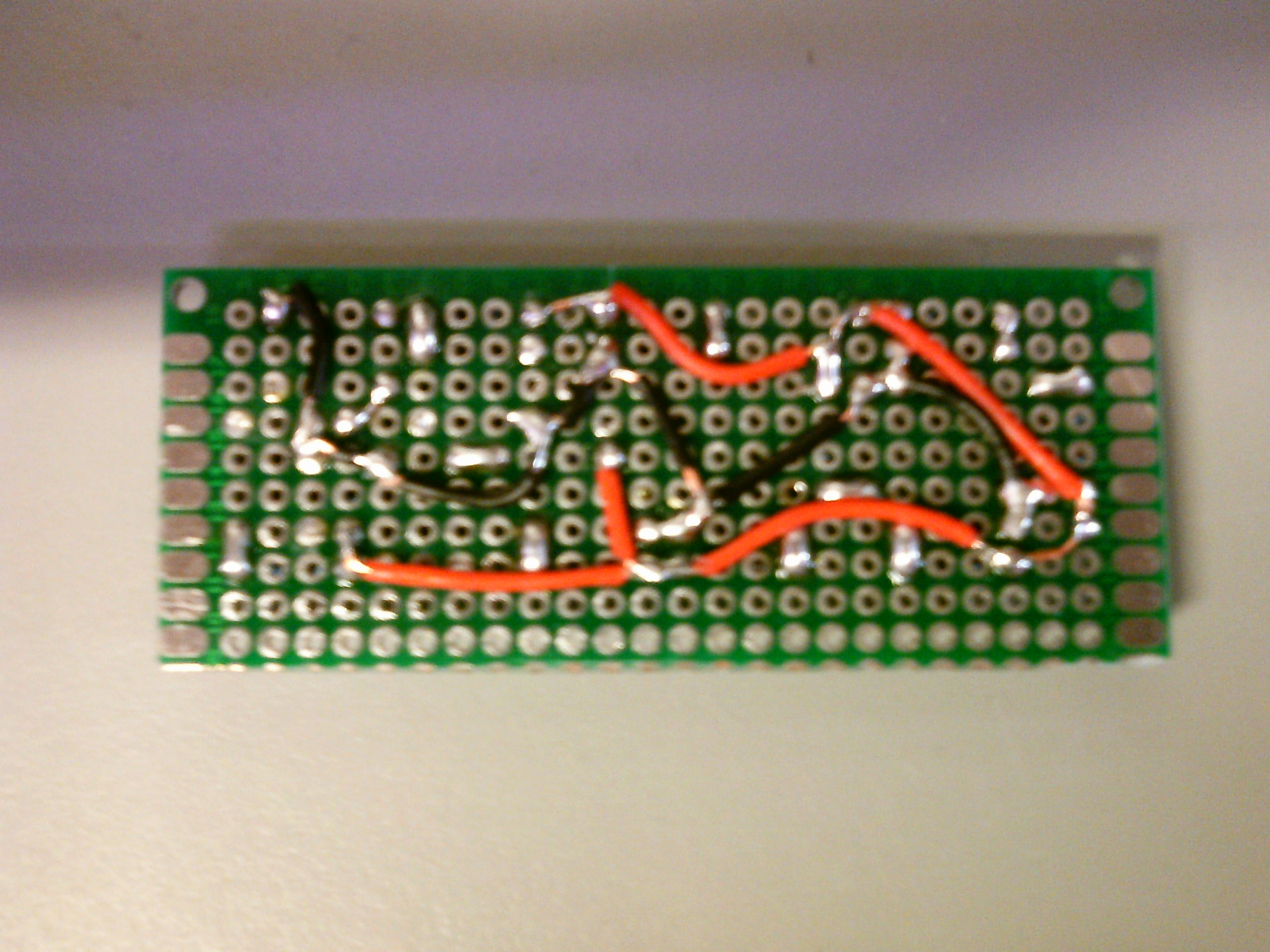 | 4,032 × 3,024 (1.86 MB) | Mahjongg (talk | contribs) | GND and VCC wiring on bottom of PCB, right hand side of picture is left hand site when the PCB is turned with buttons up, with the "cross buttons". The lower two rows of pins will be soldered to the GPIO header, with two rows of two holes on either sid... |
You cannot overwrite this file.
File usage
The following page uses this file: