The worlds smallest (S)NES emulator
| Project (S)NES emulator | |
|---|---|
| |
| A very tiny, but fully functional NES and SNES emulator based on a Raspberry PI Zero WH. Shown is the joypad PCB, which connects to the "base unit" with a long cable. | |
| Status | In progress |
| Contact | Mahjongg |
| Last Update | 2018-05-01 |
I tried to buy the recently released NES Classic Mini system on its launch day (the 11th of November 2016), but failed because Nintendo distributed just a very few systems worldwide, creating an immediate shortage. The largest game shop chain in the large town den Hague where RevSpace is located received just one New classic Mini for their two shops! Thats how thinly Nintendo distributed these things.
I studied what the NES Classic Mini was based on, and discovered it was actually an emulator based system, (not a direct hardware re-creation) based on an ARM system (a quadcore all winner SoC). It could take many weeks before I will be able to buy one, but I knew that for Raspberry PI's there exists an emulation system called RetroPI that is able to do the exact same thing (and then some more).
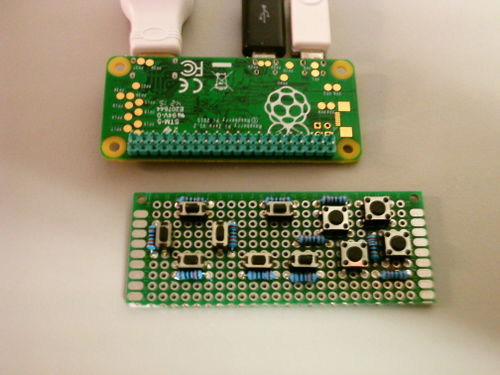
I had a raspberry PI zero left unused, and thought it would be nice to install RetroPI on it, I also knew that it would be possible to control retroPI with buttons connected to the PI's GPIO's, and a piece of code from Adafruit that converts the buttons to a "Virtual USB keyboard". Looking at my zero I envisioned that it had a shape (but not size) resembling a NES controller, and had also seen YouTube movies that described a PI zero being built into a NES controller. I decided to see if I could place the joypad buttons on a piece of perfboard that had the same size as a Raspberry PI zero, and so this project was invented, (luckily I have small hands, so this joypad isn't too small for me). I decided to put some extra buttons on the PCB, so it resembled a SNES controller, and added one extra button, for special functions, which may come out handy later, perhaps to be able to easily exit a game (later I found out that this isn't necessary). Later I also added shoulder buttons.
the best way I initially thought was to combine the button board with the PCB would not be to put the button PCB on top of the zero, but on the bottom, this would make the "stack" of the PCB's and components much thinner, so the thickness of the whole would be more similar to a NES controller (later I found out that this wasn't really necessary).
First I would wire all buttons on one end to ground, with the other end of the button wired to one 10K pullup, all the other ends of the pullups would be wired together, so they could be wired to 3.3V. Each node between a button and Pullup will be wired to a single GPIO line (one not carrying a special function). A total of 11 Buttons are available, so I would need 11 GPIO's. But the zero has plenty of these. GND and 3V3 wiring was done on the bottom of the "keyboard PCB", wires running to GPIO's will be wired on top with thine wire wrap wire with at least four different colours (different from the black and red wires of the bottom.
I am planning to first solder a wire to all nodes, then to temporary wire up the GND and 3V3 wires, then use a multimeter to see if I can control each GPIO wire, so I know the wires on the bottom are Okay before soldering the PCB's together. I will place a piece of foam as isolation between the two PCB's.
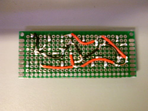
This is a picture of the wiring on the bottom of the "keyboard" PCB, showing all the GND and 3V3 wiring, and the interconnects between pullups and buttons.
note that it will be possible to also connect a full size retro NES USB controller, or a keyboard.
December 6, 2016: keypad wired up and working with RetroPI
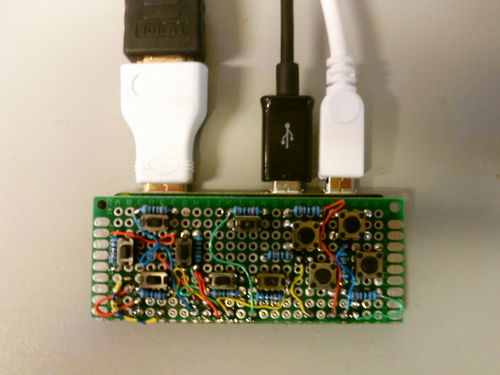
I managed to complete the wiring of the SNES compatible keypad, and got it working with RetroPI, using the Adafruit virtual keyboard driver for RetroPI, and a dedicated configuration file.
I used another raspberry PI, a B+, in the process. Installed retroPI to a 8GB SD-card with the help of 7ZIP and WIn32Imager. When that worked (with a temporary keyboard to control it) I installed the adafruit keyboard driver, using a wired ethernet connection, and re-configured the retropi.cnf file with the GPIO ports I used for the direction keys, start, pause and A,B and X and Y keys, and an extra ESC key. Then I placed the SD-card in the zero, and configured the keyboard configurator with the assigned buttons. It took a while and I made some detours, and along the way discovered I forgot to solder a pinheader pin on the Zero GPIO side that caused the up-arrow-button to not work, but in the end it all functioned. Next Job is to get some ROM images on the sd-card, so the NES emulator is activated. For that I need to create a map on a memory stick, and put it on the booted up RetroPI system, so RetroPI can created directories for the ROM's where I can put my NES game ROM's in.
the keypad will get a white vinyl cover with lettering, to cover the wiring, and a black vinyl cross for the direction keys, and white vinyl backing over the IC's and card slot on the back, all to make it neat, and make it look like a NES controller (with extra buttons).
December 10, 2016: Emulator is working
Well, it works! I can play NES games using the Joypad I built. I tried six games from the list of 30 games from the NES Classic Mini, and they run fine. However playing it isn't really comfortable, with the heavy HDMI cable hanging off the keypad. The biggest reason for that is that the keypad is really very small, the exact same size as the RPI Zero. Also the hardware is now "naked", as I have not yet covered the keypad and RPI zero on the back. That will be the next thing I will do, in the process I will also cover the buttons with red, yellow, green and blue plastic dots for the A, B, X and Y buttons, and a black plastic cross from flexible plastic on the cross buttons. I will also try a few SNES games, partly to see if adding shoulder buttons, is useful.
I'm also considering to design a small PCB, with somewhat larger buttons, so you will get a full size SNES joypad that is easy to build, it will also be possible to use a mounting structure, so you have a complete enclosure around the joypad. Finally I will try adding a composite cable to see how well the emulator works with a PAL resolution. If that works well, I will add filter logic to a PWM GPIO so that mono analog sound is supported. With such few and thin cables the Joypad will be more pleasant to use.
December 18
added a composite cable, and shoulder buttons. The composite cable means I now have just two light cables hanging off the Zero/Joypad and the picture quality is surprising acceptable. Shoulder buttons work, but mechanically they are unacceptable. In fact the size as is is simply too small for me, and real gaming is awkward on this prototype. I really wanted to play these games, so I bought a "real joypad", a SNES30 from 8bitdo, but at €50, it was not exactly cheap, and it was hard (convoluted) to get it working. I think that I can do a better job with a PCB, and better buttons spread out to a similar size as the SNES30 joypad, and finding a solution for the still awkward cabling problem. I also need a better housing for proper shoulder button support.
January 17, 2017
My employer donated a few suitable enclosures to me, with a promise I could get a few more when I wanted. I have now mounted my contraption in such a case, and added acceptable shoulder buttons. It works fine and is mechanically much stabler. Although the buttons are a bit on the low (small) side to protrude through the plastic, its still acceptable, as I discovered I could remove all pull up resistors without negative side effects, this meant that the PCB could be glued closer to the plastic, meaning the buttons protruded higher above the surface of the enclosure. They are still somewhat small and cramped together though.
I also have added analog sound, by using the option to switch the PWM used to generate analog audio from the other PI's, to a set of (or a single for mono) GPIO pins, (which I was glad to see could be accomplished with a single line in config.txt) and adding my own "filter circuit".
This means I now have a usable setup with just three cables, one for audio, one for video and one for power.
Sound works fine if you turn up the audio settings in Retropie to the max. The software needed for direction PWM to GPIO's is just one simple line you add to config.txt, if you then connect a HDMI cable you still get HDMI audio and video automatically! Also the Video (which is NTSC I presume (no its actually PAL!)) works great, much sharper than an original NES. Perhaps I can switch the video to PAL, for an even better picture (its already PAL, as most monitors I tried work fine).
I'm now planning to design a small PCB that fits into this enclosure, and plan to use switches with long stalks, so that I only have to drill circular holes into the enclosure, so I don't have to make irregularly shaped holes in the case, which is a lot of work.
I'm planning to use thin four pole cable, with wires for 5V, GND, Video and Audio, which are wired to a very small PCB at the end which contains just a regular USB type B connector, and two RCA connectors, this can then be placed in a sub miniature copy of a NES. The cable doesn't have to be much thicker than a normal keypad cable.
January 18, 2017
Started on PCB design (with Ultiboard) created shape of PI-zero with GPIO pins and video pins, schematic symbol, and PCB shape. Also looked at an alternative enclosure that can be bought (the one I got could no longer be bought). Decided on PCB board size that fits in this enclosure and possible future one that is 30mm high, and 90mm wide. Thought about stereo sound, which needs an extra wire, but could be optional. Wire should be connected permanently to both controller and interface for simplicity, but I could use 1/10" header pitch connector for low cost, and possibly (to still add more connections) a 2x3 pins connector (later on I decided against this idea, and switched to a RJ-12 modular connector. I still have to choose buttons that are cheap but reliable and usable. Decided the PCB will be on the topside of the Zero for ease of layout (don't have to rotate the design in my head) and to protect the electronics beneath it. Use of single sided board is possible with copper layer on top side so you can solder the header on top, switches with PTH or SMT pins can be soldered on top, and filter components can be placed in between Zero and PCB (on underside PCB) when using PTH components, or on top when using SMT.
As single sided boards normally have copper on bottom, but my board needs copper on the top (so I can solder the pinheader pins, So I may have to mirror the layout afterward, or check gerbers/drillfiles carefully before ordering PCB's. If price difference isn't too big dual-sided PCB's might still be better for better mechanical reliability. I would prefer to Use PTH components ONLY for ease of build. So don't use micro-USB connector, but regular type B (square) connector. If PTH components on bottom are a problem, I might have to switch to SMT, but Ill use components that have a manageable size (1206).
February 7, 2017
I had built a version of my "NES console" prototype that used a single 4-wire cable, to a "micro NES" at the end, which is housing just the three connectors needed, an USB Type B power input, and two RCA output connectors, one for video, and one for audio. That worked, but I wasn't satisfied with it as the sound sounded awful, lots of hum, and switching sounds, and if you looked carefully you could also see intensity faults in the video signal.
I decided that combining the power and signal ground wires was a bad idea, and decided that adding a fifth wire was a necessity. So I made the change to try my theory, and also added a "connector" to the "micro NES". I am now considering a 6-pin modular jack,using six wire telephone cable for the final design, but for the prototype I used a simple six-pin angled pin header to female header structure with 5 wires, and that worked fine. I used a six pin angled header, so I could cut off the second pin of the six, and glued close the second hole in the corresponding female header, for reverse insertion protection. The 5 wire "cable" was made from a strand of band cable with 5 wires, which is cheap and works fine. Length was about 1.5 meter.
The result literally left nothing to desire, picture and sound are now excellent (for PAL composite video and Mono analog audio, that is).
Now that it works perfectly I feel that my prototype is finished, and I can start at designing the PCB knowing that the result will be satisfying.
February 14, 2017 prototype finished
Here is a picture of the finished prototype gamepad, which is actually the whole NES emulator, consisting of a Raspberry PI Zero with a support PCB for buttons and some analogue filters for audio. Power input, and AV output is connected through a 5-wire cable to the "NES console", which houses the USB-B 5V 200mA power input connector, and two RCA connectors one for audio, and one for PAL video.
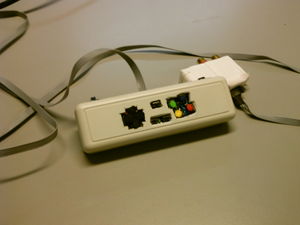
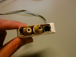
To the right is the prototype "micro NES", at the end of the cable, which is extremely small, as it (almost) only consists of the power and A/V connectors.
These pictures show the prototype, the final version will have a PCB for the various A/V/power connectors (an USB-B connector for power, and three RCA connectors, one for video, and two for stereo audio) in the "back", and a single RJ-12 (6P6C) modular jack connector on the front, so you can (dis)connect the gamepad to the "NES", with six wire modular cable. The sixth wire means I can also add stereo capability. I will make 4-wire cable capability optional, when you add a wire link to the PCB to combine power and signal GND, and restrict to mono audio, but this is not recommended.
February 14, 2017 Now working on the PCB.
I started working on the PCB, with all the new ideas I gathered from the prototype.
February 28, 2017 Modifications to accommodate the PI Zero W.
To accommodate the new version of the Raspberry PI Zero W, and specifically its plastic case, I decided to come back from my decision to put the keypad PCB on top of the Zero, I realized that I could use the new enclosure, but it would be nicer when the keypad PCB would be rotated so that it could be mounted on the flatter back-side of the Zero. So I revised the component placement. This does mean that the pin-header connection between Zero and keypad PCB should be dis-connectable, as with the PCB soldered directly to the Zero the zero can no longer be removed from the case, and that means you cannot remove the SD-card from its holder (unless you make a hole in the case). This is doable with low profile female headers, and compatible pin-headers.
Its also possible to still fit the PI, and keypad PCB with a directly soldered PCB inside the originally planned enclosure.
With the new Wireless variant of the Raspberry PI zero, it is now possible to scrape for album art, and to upload content directly wirelessly. It is also possible now to use a wireless keyboard, and a wireless Joypad, such as the 8-bit DO (for a second player).
I also made last minute changes to the schematic based on the latest insights (switched the two audio channels to simplify the layout).
The schematic can be downloaded here:
File:Emulator schematics.pdf
March 7, 2017 printed the component setup, and modified it to look more like a real SNES controller
I had printed out the Gerber plot of my previous component setup and board size and compared it to a real SNES joypad. My conclusion was that the button placement was still far too small, and a larger size PCB was possible and necessary.
I noted that the enclosure, that I have about a dozen pieces off, was about the right width but not height compared to the real Joypad. I measured up the size of a PCB that would fit in it, and the location of two 5mm pillars for screws, for which I had to create holes in the PCB, tho other plastic structures I could cut away, but not the pillars for the screws.
I modified the size of the PCB, so it would fit in the case, and added the two holes in the right places. I spread out the buttons so their positioning more closely resembled that of the original, and made a new Gerber file to check the new positions and PCB size.
March 14, started with PCB layout
Started with layout work, trying to fit it all on a single sided board, making use of the fact that switches can also be used as "jumpers", which is a bit tricky. Its also hard to route it all on a single sided board, need to use my "bag of tricks". However its a nice challenge and will keep the cost of the PCB down. I will try to route the important traces (video + video GND) the shortest. Need to remember to add 4 mounting holes for a piece of perspex over the switches, which could also be used to replace the case. At the end of the evening I had managed to do a large part of the layout work, when someone found it necessary to switch off the power, and as my laptop doesn't have a battery I lost some work, (just 15 minutes or so, as I save often).
March 21, PCB Layout finished
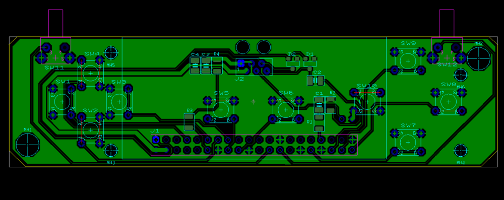
Finished the layout, it looks like this:
Note, this is a single sided PCB, all copper is on the TOP-SIDE only! I have used the fact that the button pins are connected along the long axis to each other, where I use to make connections, (Bridges) the connection is marked with a red line.
All capacitors and Resistors are easy to solder 1206 size, while the dual diodes are equally easy to solder SOT23's.
This is the schematic: File:Emulator JOYPAD schematics.pdf
Next up, the schematic and PCB for the "console" with the power and AV connectors.
March 22, PCB checks out fine
I've uploaded the PCB to my favorite PCB manufacturer Eurocircuits, to see if they could make them (if there are no violations of their production rules in it). This is the preview I got from their checkout program, but note that I will probably NOT use them, as they ask about €7 per piece for them, which I think is much too expensive. Also I will wait until I also have the other "console" PCB ready, so I can "panel" the two together.
March 25, also designed the console part
Modified the schematic to also include the console part, with three RCA (Tulip) connectors for Stereo Audio and Composite Video, an USB Type B (square) USB Power input, and an RJ-12 (think 6-wire telephone jack) connector). And also added the "console" part as a break off part to the main PCB. Pictures coming soon. P.S. I have had the idea to add 1mm holes in the PCB at the center of each button, so the PCB can be used as a drill template for the holes in the enclosure, so some traces have to be modified to make place for these holes.
March 29, Finished PCB with "console" part
Here is an artist impression of the finished PCB:
April 4, 2017 Renamed to RETROPAD
I decided to give my RETROPIE JOY-PAD the name "RETROPAD". Finalized the PCB layout and schematics, generated production files (Gerber and Drill Files)
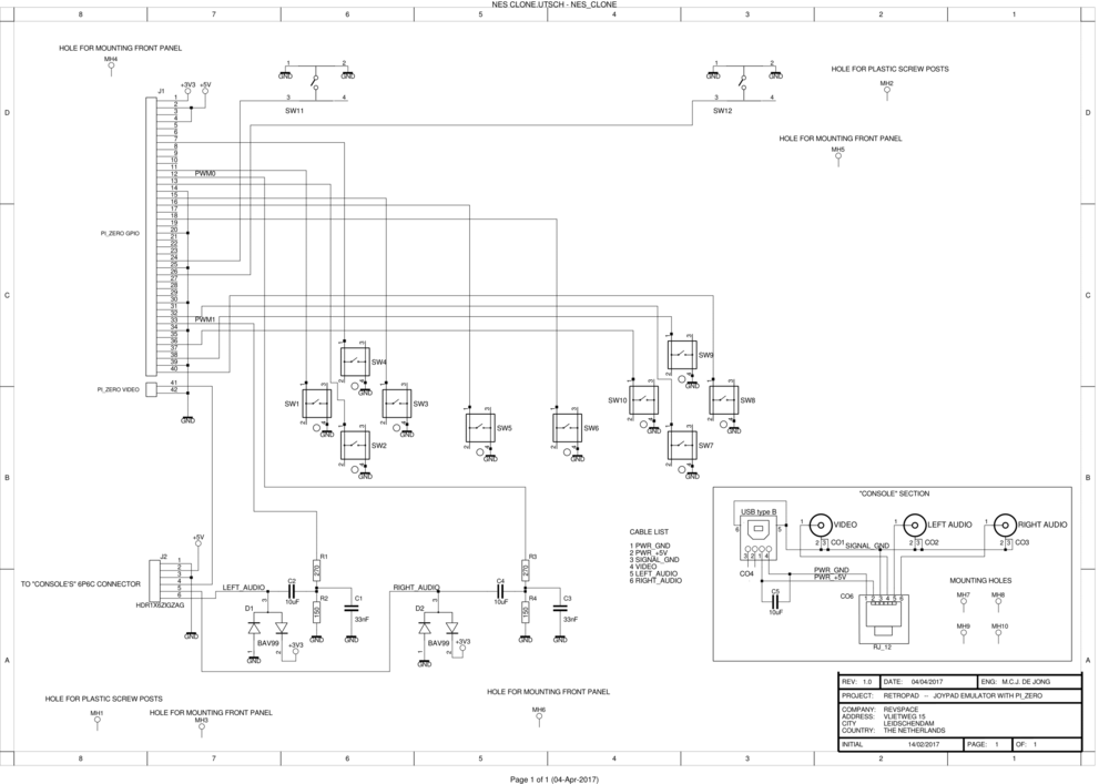
This is the final schematic:
April 10, 2017, Tested PCB layout for producibility
Uploaded my new combined PCB design to a PCB manufacturer to test for errors, and found it did contain two overlapping drill holes (in the break off via rows, the silk screen text has the text "Break Here" and an arrow pointing to the two pair of holes that are overlapping), and it also reported the absence of some needed data in the gerber files, probably indicating I used the wrong type of gerber creator. Still the preview pictures is nice, and I don't want to keep it from you, so here it is: See updated picture below.
April 13, 2017, final rename to RETROPIPAD
Decided the name RETROPAD was too common, so changed it to RETROPIPAD (as in "RETROPI based gamePAD"). corrected small layout errors, and uploaded the gerber files again to Eurocircuits to check for layout errors, made a new preview, and updated the old picture to this:
Decided to open source my design, and make it more SNES JOYPAD like
September 2017 Planning to do some changes to make it more SNES like
I want to do a redesign the RETROPIPAD using the newer more future proof KICAD CAD system under Linux I have now started to use, and at the same time I want to use slightly larger ABXY buttons that can use coloured plastic top caps. This because it seems interest in the SNES mini is now growing, and the Raspberry PI Zero can also emulate SNES games.
I have acquired data about somewhat larger buttons for which you can buy key caps in various primary colours, which I'm going to use in this more SNES oriented re-design. I finished large parts of the schematic in KICad, drawing the schematic in a style resembling the relative positions of various components on the PCB.
October 11, 2017 Redrawn the Schematic with KiCAD
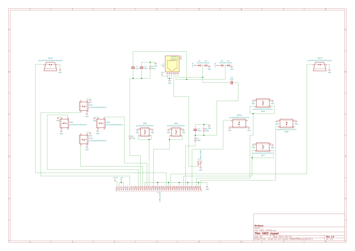
This is the new schematic, drawn in KICad. File:SNES JOYPAD.pdf I also started on component placement. Note that this schematic reflects the actual placement of all the components, also this version uses 12x12mm buttons for A B and X Y buttons, which support colored key-caps.
October 18, 2017 Finished KiCad component placement and board dimensions
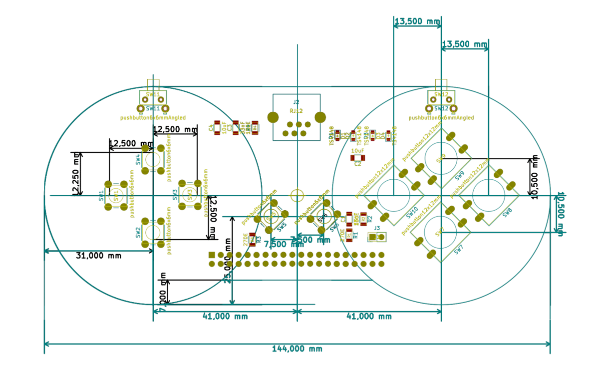
See: File:SNES JOYPAD PLACEMENT with dimensions.pdf
October 24, 2017 Figured out how to construct the board shape, and create gerber and drill files
Today I made final placement corrections, and constructed the board outline, using circle segments, which was quite tedious as KiCad uses a convoluted way to do so, which made it very difficult to construct a board outline where line segments are actually contiguous. In fact I could not reach the absolute precision that KiCad wanted (when trying to show the board size in its 3D simulation, it complained it could not determine the board size because line segments did not make a "closed figure"), but I considered it would be good enough for PCB manufacturers. So I figured out how to make "production files" (gerber and drill files) and uploaded them to my favorite PCB manufacturer, (Eurocircuits) and this was the result:
So I guess its working :-) .
I can see a few problems in the provided component footpads, the RJ-12 connectors holes for the plastic pins are wrong, both in location and size, and also the holes for the pins of the 12x12mm (larger) keys seem a bit too small, so I need to learn how to edit (and create my own) footpad models. I was lucky enough to find existing footpad models in KiCad's footprint (and schematics) library so far, but at one point I will need to create my own models.
Also looking at the ratsnest in the PCB layout, I seem to be missing a lot of connections, so perhaps that another problem I have to solve. p.s. looking at the missing rats nest connections, I see that the all seem to be connections to buttons, and all buttons have in common that there are two nodes (lines in the netlist) for echo button, and so also two rats nest connections, the short ones I see (the one from one pin of the connector to the other). So I can imagine that perhaps the rats nest shows only the shortest connections (one I still have to make). but I can do that! If I make the dummy connection on the backside (as as single sided PCB I will not plot the backside, so I can use it for virtual connections, created by the buttons themselves) then perhaps the long rashest line will show up. thats not how it should work, but I can live with that. we will see...
November 1, 2017 Netlist problems!
Tried to route the short connection between button pins, but it didn't help! The long connections did not start to show up, they also did not show up when highlighting a net. It seemed the connections were simply not in the netlist, even after regenerating, and reloading it. It seems to be some strange bug in KiCad, perhaps related to the fact that the keys have several pins with the same labels!!! I need to solve this problem before I can continue, but not today...
November 8, 2017 Netlist problems solved!
The netlist problems where due to the fact that there were bugs in the definition of both the 6x6mm and 12x12mm buttons. The pins of these schematic symbols were drawn with their connecting points on the inside of the pin, instead of the outside of the line that represented the pin. Therefore drawing a wire to the outside of the pin-line didn't really make a connection, which I noticed when I tried to drag the component, a TIP from a KiCad user I met at Awesomespace, thanks for the TIP Michai ! I did not bother to try to fix the schematic symbols, but instead I simply drew a wire segment over the pin to the inside of the pin, where the wire connected with the pin. That worked, and after that the netlist was fine.
The next problem was that the existing RJ-12 connector in the library was useless, it seemed to be a connector where you plug in the jack from the top, instead of right angled (from the side), so I defined a new RJ-12 connector, in my own library. Only to find out that initially it was impossible to assign the footpad to the schematic symbol... It took me some time to find out that with the footpad wizard I could add my library to the main library. whew... Then I noticed that the pin-numbering 1 to 6 was reversed, so I corrected the schematic symbol, and removed the pin-7 and pin-8 which no longer exist, as pin-7 and 8 no longer are copper plated holes, but just 3.2mm unplated holes.
Now I could try to route the traces, and with some effort I managed to gain 100% connectivity (I routed all traces) including GND! With GND often being routed through the connector (which connects two pairs of pins). So again, it cn be a single sided PCB. I didn't want to try to add a ground-plane just yet, that is still a bridge too far! Especially because I will probably add some unplated holes for mechanical purposes. It will probably work just as well without a ground-plane especially if I widen some ground traces.
I have to remember to increase the size of the holes of the 12x12mm buttons, which I'm sure are too small. Also I think I will try to change the footprint of the sideways (shoulder) buttons, as the current footprint only supports buttons that are a bit expensive.
November 15, 2017 designed "console system" for SNES JOYPAD
Also designed a separate PCB for the "console" with the power input and audio and video outputs, as with the first version, it is connected to the joypad with a six-wire cable with RJ-12 modular connectors (used, among other things, by a telephone handset). here is the .PDF: File:SNES JOYPAD BASE.pdf.
and a picture: 
Most of the work was designing the footpads for the "CLIFF" PHS-2A (FC6837) RCA connectors, you can buy from Conrad for €0.60 [1]. Strangely enough there seems to be no real standard for such RCA connectors, most have different footpads, this version is a bit easier to use and much cheaper than the one I used in my ZX81 clone.
November 21, 2017 changed my mind about RCA connector footpad
The situation about the RCA connector footpads not seeming to have a standard irritated me, and I decided to study it a bit more; these are the conclusions I drew:
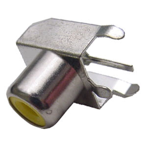
- The first RCA "right angled" PCB mounted connectors seemed to have been "all metal" devices, only having a plastic isolation bus between the inner cylinder and the outer "barrel", and having three mechanical mounting pins, one in the middle front, and two in the back, all with 200mil (0.2" or 5mm) distances between the three 2.6mm to 3mm holes, providing support for the U-shaped main body to which the barrel shaped outer cylinder was mounted, with the signal pin (connected to the inner cylinder) connected to a pin ending roughly between the two back mechanical mounting holes, with a somewhat smaller pin. Most often in a circa 1.6mm hole.
- Sometimes the middle hole was moved a bit (a few mm) toward the front.
- The 2.8 mm pin on the front, was normally moved a bit back from the "bottom of the U-shape" so that the U-shape could be flush with the PCB edge without the hole being through that edge. sometimes this was ignored and the hole was directly under the front edge resulting in a hole 8 mm (not 5mm) from the two back holes.
- later versions with a body made from plastic were designed, and the idea came that you could make a version that had a switch built in that disconnected the audio from a second pin when an RCA plug was plugged in, so that (for example) an internal speaker was automatically turned off when connecting RCA plugs. An idea probably borrowed from DC barrel power inputs which normally have such a switch (for mechanical reasons in the (GND) wire of the power connector) so that plugging in a DC source would automatically disconnect internal batteries. Such a design needed two pins, so the designers of such a connector used the two back (mechanical mounting positions) as audio input + switch output connections, but kept the middle front hole as the GND pin.
- Later versions were made without the switched output pin (normally the left hole seen from the front) so they only had a pin for the right hole.
- Some switched versions brought the back two pins closer together, about 7.5 mm instead of the 10.5 mm normally used, probably to distinguish them from the older ones, and so avoiding them erroneously being mounted into a PCB meant for the non-switched older versions.
- the older full metal versions are often far cheaper, like 60 cent instead of the €2 that plastic based ones with a built in switch are typically sold for.
I decided to adopt the older cheaper full metal versions, with a middle (signal) pin with a slightly larger (2.0mm) hole placed a millimeter toward the front, between two mechanical 2.8 mm support holes (not connected to GND) and with two GND pins one 5mm from the back, and one 8mm from the back, both 2.8mm. I hope this footprint will support most "non switched" full metal RCA right angled connectors, as well as most plastic versions that are based on the non switched design, which often have just two pins, the GND pin, and a signal pin 5mm further to the back. These are often sold with white, yellow and red isolation buses, and are reasonably low priced. Although the cheapest ones just use white or gray or black plastic. Which is fine if the hole in the case is labeled instead of using the color coding.
Typical connectors that should fit the PCB are the CLIFF FC68391, the KLP 0848A-2, the RCJ-01 and the ECON 1303833 and many others. If a user decided he needs to mount a switch based connector, he can still do that by soldering a wire between the (unused) middle signal hole, and the right 2.8mm back hole.
I have designed the PCB, and created Gerber and drill files.
This is a picture of the board, left topside, right solderside.

finished layout SNES JOYPAD revision 1.0
and uploaded gerber/drill files to https://comfy.moe/dpjyxu.zip Here is a picture of the PCB:
January 15, 2018 The Launch of the Raspberry PI Zero WH warrants a re-design
Today the raspberry PI foundation launched the PI Zero WH, a Zero W with pin-headers soldered in at the factory. This warrants a re-design for reasons I explain below.
My original reasoning was that as the PI Zero did not have any pre-soldered headers it didn't really matter on which side this board would be mounted, as the headers needed to be soldered in by the user anyway. Now this is no longer true, and so it has become possible to develop a product that can be simply plugged onto a Raspberry PI WH, instead of a kit that the user had to (at least partly) solder together himself. Were it not for the fact that I stupidly had designed it to be "soldered directly onto the back" to keep it low profile..
Now I see that that was the wrong decision, and so I have decided to re-design the board so that the GPIO connector is rotated and mirrored so that the board can be plugged on TOP of a Raspberry PI WH, probably that means that I have to re-shuffle the GPIO's used so that the layout doesn't become much more complex. And I have to re-write the GPIO configuration file.
February 20, 2018 Created a schematic for the version for Zero WH
The schematic for the new version with GPIO's swapped is File:SNES JOYPAD WITH ZERO WH.pdf The assignment for GPIO's of this version is now (experimentally):
Pin 7 Right shoulder
Pin 11 A
Pin 13 B
Pin 15 X
Pin 16 Y
Pin 18 Select
Pin 24 Start
Pin 26 Right
Pin 32 Down
Pin 36 Left
Pin 38 Up
Pin 40 Left shoulder
Pin 12 is "left audio"
Pin 33 is "right audio"
note that the same GPIO's are used as originally, they are only re-assigned
note that the zero WH will be rotated so that pin 1 (the square pad) of the 40-pin-Pinheader will now be bottom RIGHT
27 March 2018, finished the layout for the Zero WH version
Managed to complete the routing, now also added two 2.5mm mounting holes to mechanically mount the PCB to the zero, and added four 3.2mm holes to connect the PCB to a "top plate" with holes for the 10mm buttons, and holes for the smaller buttons, and a cross shaped D-pad. Have to figure out how to create non round cutouts in this top plate (which is designed as a PCB) in KiCad. Have started on the top-plate (PCB) too. The optional top-plate would cover up the buttons underneath (with the button caps sticking through), as well as making a cross shaped (3D printed) D-PAD possible. for a more professional look.
I also want to design a NES or SNES shaped housing, either laser-cut or 3D printed. Perhaps my nephew Wouter can help with that, I'm considering making it a bit larger than the current PCB would suggest, as its now probably too small (and a bit too light).
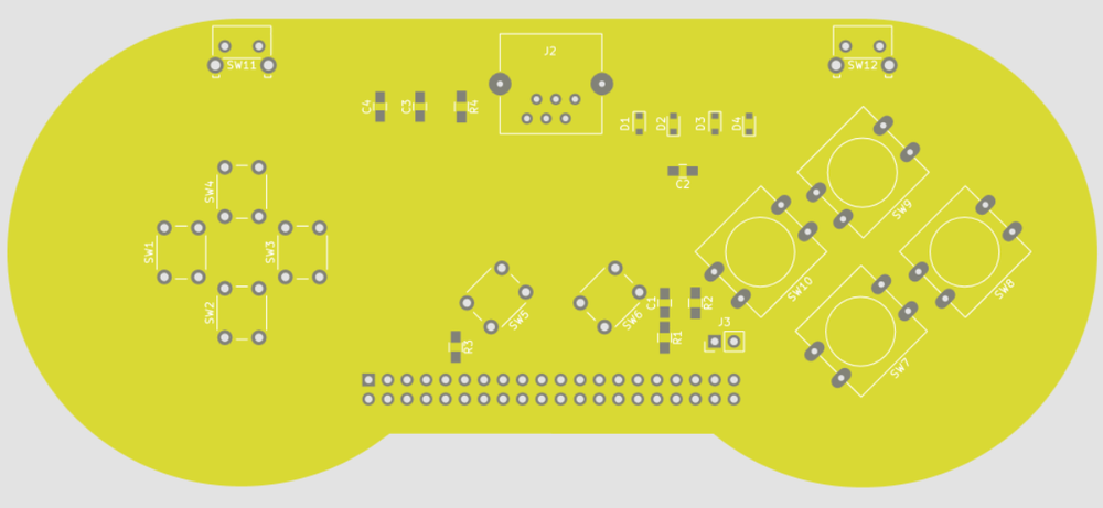
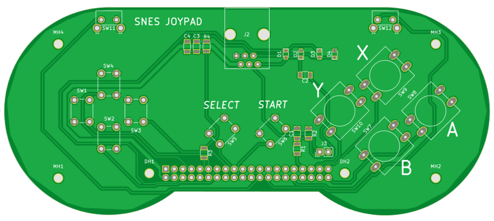
This is a new picture of the SNES JOYPAD WH (for the zero WH).
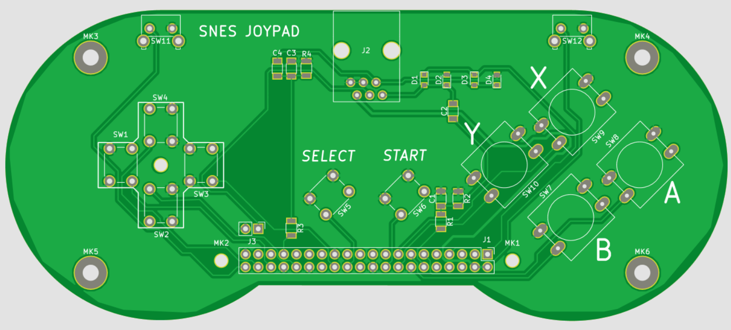
I have also designed a cover plate for it to mask the components and wiring underneath, and that keeps the buttons and D-PAD in place.
30 April, 2018. add mounting holes for shoulder button "shoulders"
As is no the "shoulder buttons", are just that, buttons, hanging off downwards from the main PCB. I have to rethink if I cannot place real (plastic) shoulders between the main PCB, and the cover plate, perhaps there won't be enough room between the PCB and the cover plate to accommodate the height of the actual buttons, I will have to see what I can do about that. Note that the "normal" angled push-buttons that I intended to use are about 7mm high.
In principle, the distance between top of the PCB, and bottom of the top plate should be around 8.0mm, according to my estimations, so the angled buttons should fit... I will add two screw holes to mount shoulder-buttons with self tapping screws, hole diameter 3mm, screw heads 5.5mm, so two 3.0mm holes 5.5mm apart.
