ZX81plus38 simple to build ZX-81 clone
| Project ZX81plus38 | |
|---|---|

| |
| Most people I showed my ZX-81 clone (ZX81+35) said they liked it, but with such a tiny board and with so many "difficult" surface mount components, they they doubted whether they would be able to build this kit, so I restarted my effort, to try to build a 100% ZX-81 clone that anybody could build, with commonly available parts. | |
| Status | Initializing |
| Contact | mahjongg |
| Last Update | 2019-09-29 |
September 18, 2019 I started the design
For now I will call it ZX81+38, but I doubt it will be finished in 2019, so it will probably be renamed to ZX81plus39... :-)
I started analyzing my current schematic, to see whether it contains components that are not available in PTH, and unfortunately there are some, for example "unbuffered inverters" (74HCU04) used in the crystal oscillator, are no longer available in DIP. Also some other logic isn't available in DIP, 13MHz crystals are hard to get in PTH versions, and 6.5MHz are not available at all. I decided to switch from 128K flash ROM to 32K OTP ROM's because the latter are available in DIP-28, while for the former I MUST use a PLC-32 socket. Eproms are a few dimes more expensive there days than OTP's, but DIP sockets are much cheaper than PLCC PTH sockets, and OTP and RAM in DIP-28 placed next to each other are much easier to layout. I also found cheap 32K x 8 static RAMs, also in DIP-28, which will be easier to layout for.
I will design it with KiCad unlike the older version which was designed using Ulticap and Ultiboard.
September 20, 2019 made a preliminary component placement of connectors and drill holes
Measured up a real ZX-81 PCB, and determined the size of its PCB, the locations of its mounting holes, and various connectors, I noticed that the Z80, and its ROM and RAM needed to be in a particular orientation, because of the mounting holes. determined the positions of the Video out connector (although the standard RCA output plug sits lower to the PCB than the RF-modulator output), and determined where the 3.5mm jacks for EAR and MIC should be located. For DC input I did not use another 3.5mm jack, nor did I choose a barrel jack, instead I used a model B (square) USB connector, so you can power the ZX81+38 with an USB charger and a type-A to Type-B (Device) USB cable.
I also placed the expansion port connector, which has the normal contact fingers, but can be enhanced with (gold plated) an angled dual row pinheader connector, so you can choose compatibility, or a more stable connection. I will route to the edge connector, and will place the edge connector "fingers" manually from there.
September 24, 2019 I placed most of the components in the schematic
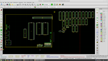
I was curious if my USB replacement logic would fit, so I quickly placed most of the needed logic in the schematic, and annotated them the same as my SMT version (logic simplification and renumbering will come later), and gave them PTH footprints. At the end of the evening I had enough of the schematic elements to do a forward annotate, so I could do an estimate of it would fit, the result is visible in the top right hand corner of this page. To my relief I found that it should fit (its just a rough estimate obviously).
September 29, 2019 continued with component selection and routing of the schematic
I found out which combination of gates and such resulted in the fewest physical IC's, swapping some gates around, and trying to find replacements for single gate IC's, which do not exist in DIL. changed the AND that combined HSYNC and VSYNC to and EXOR as during VSYNC HSYNC pulses actually appear as inverted in the VSYNC signal, but perhaps I should check my logic here carefully.
I also changed the AND combining video with the nPORCH into a NOR, with inverted inputs, also something to check later.
here is a preview of the schematic so far. File:ZX81plus38.pdf