ZX81plus38 simple to build ZX-81 clone: Difference between revisions
| Line 103: | Line 103: | ||
[[File:Placement and ratnest 2019-11-20 02-05-42.png|1000px]] | [[File:Placement and ratnest 2019-11-20 02-05-42.png|1000px]] | ||
note to self: R23 can't stay where it is, it conflicts with the DB9 connector. | |||
Revision as of 16:11, 20 November 2019
| Project ZX81plus38 | |
|---|---|

| |
| Most people I showed my ZX-81 clone (ZX81+35) said they liked it, but with such a tiny board and with so many "difficult" surface mount components, they doubted whether they would be able to build this kit, so I restarted my effort, to try to build a 100% ZX-81 clone that anybody could build, with commonly available pin-through-hole parts. | |
| Status | Initializing |
| Contact | mahjongg |
| Last Update | 2019-11-20 |
September 18, 2019 I started the design
For now I will call it ZX81+38, but I doubt it will be finished in 2019, so it will probably be renamed to ZX81plus39... :-)
I started analyzing my current schematic, to see whether it contains components that are not available in PTH, and unfortunately there are some, for example "unbuffered inverters" (74HCU04) used in the crystal oscillator, are no longer available in DIP. Also some other logic isn't available in DIP, 13MHz crystals are hard to get in PTH versions, and 6.5MHz are not available at all. I decided to switch from 128K flash ROM to 32K OTP ROM's because the latter are available in DIP-28, while for the former I MUST use a PLC-32 socket. Eproms are a few dimes more expensive there days than OTP's, but DIP sockets are much cheaper than PLCC PTH sockets, and OTP and RAM in DIP-28 placed next to each other are much easier to layout. I also found cheap 32K x 8 static RAMs, also in DIP-28, which will be easier to layout for.
I will design it with KiCad unlike the older version which was designed using Ulticap and Ultiboard.
September 20, 2019 made a preliminary component placement of connectors and drill holes
Measured up a real ZX-81 PCB, and determined the size of its PCB, the locations of its mounting holes, and various connectors, I noticed that the Z80, and its ROM and RAM needed to be in a particular orientation, because of the mounting holes. determined the positions of the Video out connector (although the standard RCA output plug sits lower to the PCB than the RF-modulator output), and determined where the 3.5mm jacks for EAR and MIC should be located. For DC input I did not use another 3.5mm jack, nor did I choose a barrel jack, instead I used a model B (square) USB connector, so you can power the ZX81+38 with an USB charger and a type-A to Type-B (Device) USB cable.
I also placed the expansion port connector, which has the normal contact fingers, but can be enhanced with (gold plated) an angled dual row pinheader connector, so you can choose compatibility, or a more stable connection. I will route to the edge connector, and will place the edge connector "fingers" manually from there.
September 24, 2019 I placed most of the components in the schematic
I was curious if my USB replacement logic would fit, so I quickly placed most of the needed logic in the schematic, and annotated them the same as my SMT version (logic simplification and renumbering will come later), and gave them PTH footprints. At the end of the evening I had enough of the schematic elements to do a forward annotate, so I could do an estimate of it would fit, the result is visible in the top right hand corner of this page. To my relief I found that it should fit (its just a rough estimate obviously).
September 29, 2019 continued with component selection and routing of the schematic
I found out which combination of gates and such resulted in the fewest physical IC's, swapping some gates around, and trying to find replacements for single gate IC's, which do not exist in DIL. changed the AND that combined HSYNC and VSYNC to and EXOR as during VSYNC HSYNC pulses actually appear as inverted in the VSYNC signal, but perhaps I should check my logic here carefully.
I also changed the AND combining video with the nPORCH into a NOR, with inverted inputs, also something to check later.
I had forgotten how much trouble it is to get the connections of the Z80 databus to the NOP enforcer, and pullup resistor pack right, probably I will need lost more wire swapping action to get a somewhat easy to route solution.Laying out this board will be an interactive and iterative process, with lots of forward annotations, and corrections in how everything is connected. I won´t swap data and address lines around for the EPROM (or we have to do some swapping of the EPROM content too, and that is not what I want). This implies that RAM lines swapping won´t happen either, as the ROM and RAM wiring is almost identical.
October 1, 2019 continued
Stupidly I lost previously placed mounting holes, that took hard work to do , because I imported a schematic that didn't have them, so the forward annotate function removed them from the board. I noticed they were gone when I looked at the preview picture. So after uttering a few choice words I have now entered mounting holes in the schematic, and once again started with their placement. Luckily I had made a 1:1 (real size) printout of the PCB WITH the locations of the mounting holes, which makes measuring up their locations a tiny bit easier. Now I also differentiated between 3.0mm holes for the screws that close up the case, and slightly smaller (2.5mm) holes for mounting the PCB to the enclosure. I also re-read some old correspondence about using an EXOR for combining HSync and Vsync, and saw that there are technical reasons why using an simple OR function will be better, So I will do that instead. I also realized that from revision 2.2 to the current revision 4.0 of my ZX81+35 the sync generation logic has had a big overhaul, that has never been tested. Also I was warned that my component placement drawing of ZX91+35 contains an error, listing U13, as a 74HC32, (OR gates) instead of a 74HC00 (NAND gates). I wanted to check if the BOM had the same error and tried to download it from GitHub, but for some reason I only got a .ZIP containing gibberish instead of the spreadsheet. Both problems I will fix soon. Also the person who noticed the U13 problem also has problems with horizontal sync not being present, and I have to investigate that too. He promised to send me one of his two build up prototypes that have this problem. on a positive note, he is using my keyboard PCB too, and it is working fine!
October 6, schematic mostly finished
Yesterday I finished placing of the mounting holes in the PCB, today I mostly finished the schematic.
Replaced main picture with the preview schematic as a .PNG picture.
October 9, schematic rev1.0 finished
Schematic finished for rev 1.0, updated schematic File:ZX81plus38.pdf, plus preview schematic pictures. Next up, importing the components in the PCB layout, and placement of the parts. No attempts have been made yet to try to support multiple types of ROM/EPROM/FLASH, like the original ZX81 ROM. But this schematic should be complete. New is my attempt to support the canonical cassette loading video bars.
October 13, 2019, schematic rev1.1 (some errors fixed, added ZX81 ROM support)
Found, and repaired some errors, when doing electrical rule checking, (non connected power supply pins, no footprints assigned, such errors). nNMI is now directly connected to A6, without a resistor in-between. Improved the way cassette input shows up as loading bars by using and AND port. Noticed many labels where the "'" (bis) marker was changed to something very similar, but resulting in no connections between various connections having a "'" (bis) sign in the label, checked all nodes with a bis marker (D0' to D7' and A0' to A8') for connectivity, and repaired the labels with a problem. Also, I corrected some labels where I used the backslash to denote in inverted signal, instead of the lowercase "n" I used everywhere else.
also found a small error in the original ZX81 schematic, which claims that the D7 signal is NOT connected through a 470 Ohms resistor, but actually, it IS! (I measured 470 ohm between pin 13 of the Z80 and pin 1 of side A1 on a real ZX-81), so the "D7" label on the expansion connector should have been written as "D7'".
Added several 3-pin jumpers so that the EEPROM socket can be configured to accept a ROM from a real ZX81, These jumpers are pre-connected, and per default configured for a 27C256 EEPROM, two of the jumpers can also be used to select one of four possible 8K images that can be contained in a 27C256, per default only the first 8K is used. Jumpers will be "virtual", meaning they will probably be mounted on the underside of the PCB under the EEPROM, and to change for a ZX81 ROM you will need to scratch through the pre-connection between pin 1 and 2.
All components are now cleanly forward annotated, so next job will be component placement.
Schematic is now revision 1.1 File:ZX81plus38 rev 1.1.pdf
October 15, 2019, finished schematic rev1.2 (functionally complete)
Added support for loading bars, using spare gates, only new part is one pull-down resistor. added some explanatory texts, changed U22 so that its wiring is optimal for keyboard column readout placement. converted the logic type to active low logic symbols where that was more logical, so its easier to follow the logic.
This schematic should be functionally complete, (if nothing unexpected happens) changes beyond rev 1.2 should only consist of pin or component swapping optimizations, and component renumbering (after I did the placement).
Revision 1.2: File:ZX81plus38 rev1.2.pdf
October 20, 2016 rev 1.3 supports 16K ROM's
I realized that some people might want to extend the Sinclair BASIC ROM, or replace it with something else, and might need a larger ROM, so I added a (virtual) jumper to enable 16K ROM's to the ROM encoder and added A13 to the EEPROM address lines. revision 1.3 with 16K ROM support: File:ZX81plus38 rev1.3.pdf
October 30, 2016 First component placement =
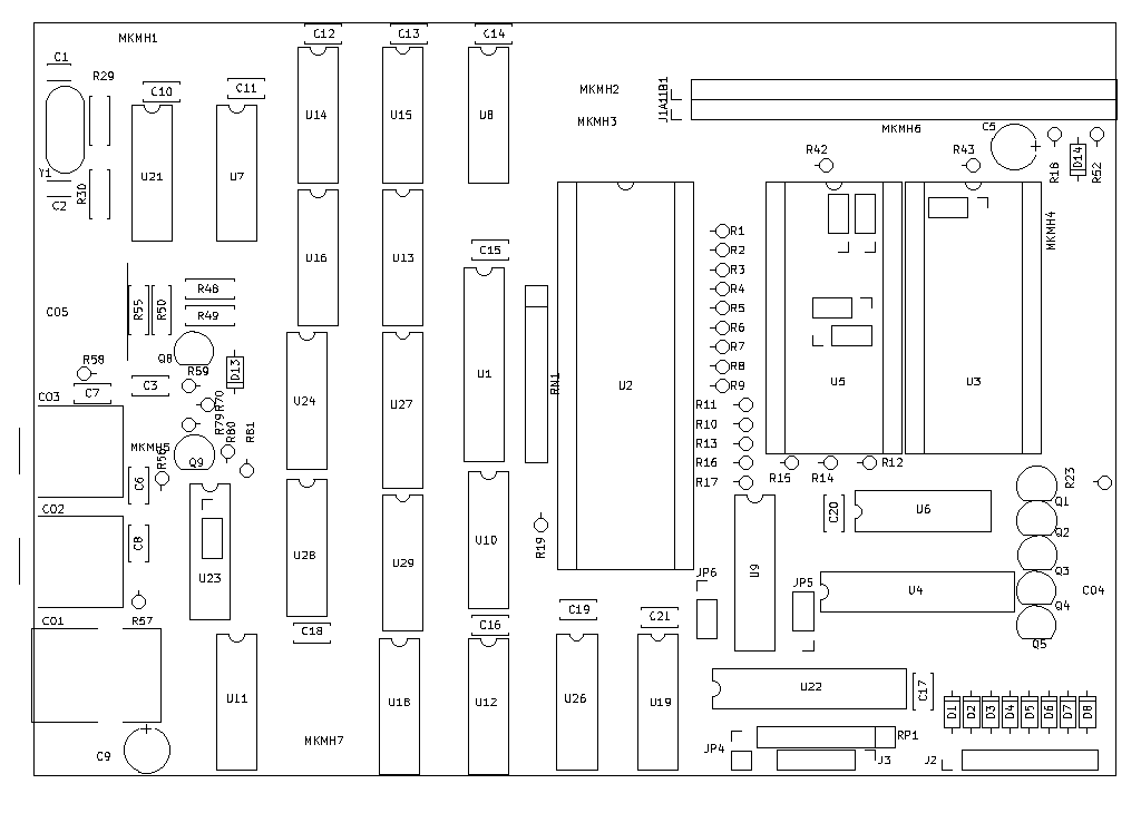
I managed to place all the components on the available IC's,but barely so.
I will probably need to do a lot of optimization (IC and gate swapping) to minimize as much as possible the routing needed, as there is almost no space left for routing.
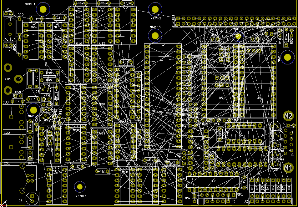
November 6, 2016 re-shaped the DIP pads to accommodate routing two wires between pads
As you can see in this picture, on various places it becomes impossible to do horizontal routing of connections, if you can only route one trace between two pads.
You can also see I modified the PADs to make this possible, I decided to use a PAD height of 60 mil (with a hole size of 35mil, and a pad width of 90mil), so there is 40 mil between two pads, for two traces you need two traces of at least 0.15mm inter-spaced with three spaces of also at least 0.15mm. So 40 divided by 5 = 8mil, or 0.2032mm. I decided to use 0.2mm traces .
Next job is to simplify the rats nest by swapping ports (and or components).
November 13, 2019 Did a lot of placement optimization
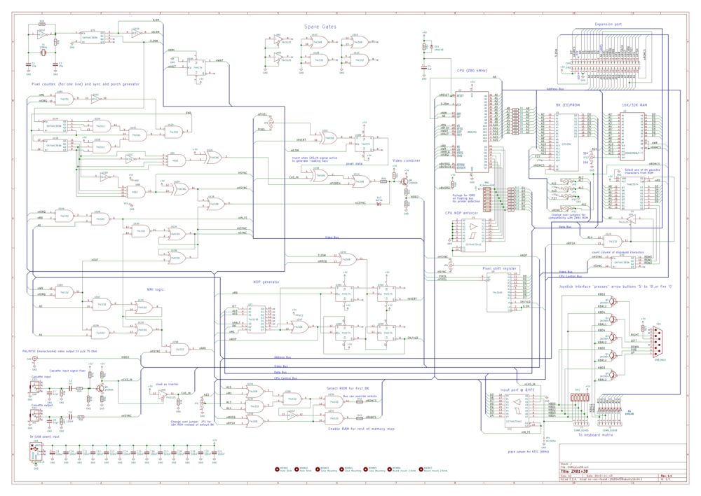
Now the schematic is updated to revision 1.4. File:ZX81plus38rev 1.4.pdf due to swapped ports.
Not only a lot of ports have been swapped, but also the component placement itself has been modified a lot.
This is revision 1.4 as a 16 color .PNG (in full resolution), open to see full resolution.
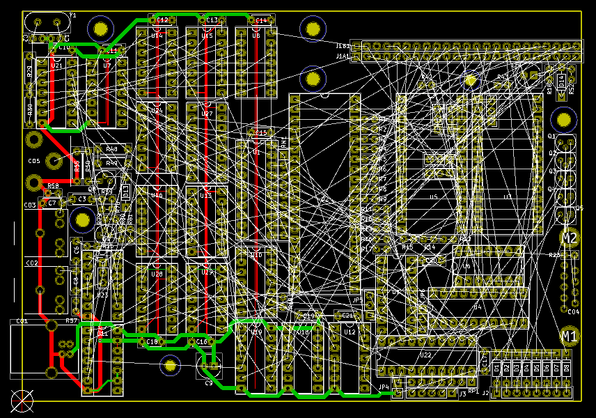
November 20, 2019 finished placement, did some power routing
based on schematic rev 1.4, I further optimized placement and started with power routing (GND and +5V) as the basis. This screenshot shows my progress:
note to self: R23 can't stay where it is, it conflicts with the DB9 connector.


