E-beam Lithography: Difference between revisions
Peterbjornx (talk | contribs) No edit summary |
Peterbjornx (talk | contribs) No edit summary |
||
| Line 4: | Line 4: | ||
|Omschrijving=Making exceedingly tiny structures by slamming charged particles into stuff | |Omschrijving=Making exceedingly tiny structures by slamming charged particles into stuff | ||
|Status=In progress | |Status=In progress | ||
|Contact= | |Contact=peterbjornx | ||
}} | }} | ||
Revision as of 12:40, 9 August 2022
| Project E-beam Lithografie | |
|---|---|

| |
| Making exceedingly tiny structures by slamming charged particles into stuff | |
| Status | In progress |
| Contact | peterbjornx |
| Last Update | 2022-08-09 |
Overview
Recipes
Resist
The resist for this DIY EBL process is quite simple:
- Cut up 4 grams of clear plexiglass (PMMA) scrap (from Lasercutter for example) as fine as possible
- Measure 96 grams of Anisole solvent in a media bottle
- Mix at 60 deg C with medium stirring for several hours until all PMMA has dissolved.
Previously acetone was tried as a solvent but it evaporates too quickly, making it too hard to get an even coat.
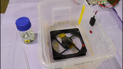
Applying it to the substrate is done by spinning it on using a modified PC fan.

This resist allows for very gentle chemistry, but there are some catches
Exposure
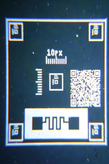
All exposures were done by using a modification to Absolute SEM allowing external X/Y input. As the microscope does not support beam blanking, vector scan is used and velocity is modulated instead of intensity.
All exposures for conductive substrates were done using 25keV electrons.
TODO (pbx): upload lab journal on parameters.
Development (Positive process)
At low electron doses the polymer gets damaged and becomes soluble in isopropanol, allowing a positive development (etch happens where resist was exposed) by washing with isopropanol at room temperature.
This requires careful selection of an electron dose that causes chain scission but not cross linking, making the exposure somewhat finnicky. The resolution is also lower.
Development (Negative process)
At higher electron doses the polymer fragments will start to crosslink and become insoluble in most solvents, meaning that acetone can be used to remove the unexposed PMMA leaving a negative image intact in the crosslinked resist.
This process should allow very high resolution, up to tens of nm.
Substrate
As we do not yet have a working evaporation coater, nor a sputter coater that can deposit aluminum, I have used space blankets as the basis for my substrate.
To prepare a sample:
- Cut a piece of space blanket to size
- Rinse the gold side with acetone until the gold topcoat is gone. Make sure to remember which side this was.
- Fix the original silver side (not the cleaned one) to a microscope slide using CA glue.
- Gently bake the sample at 100 deg C until all solvents are gone and the glue is cured.
This leaves a stackup of
- Aluminum
- Mylar
- CA
- Glass
Etch
The developed resist can be used to pattern aluminum by using an aluminum etch mixed from
- 80 % H3PO4 (starting with 85% solution)
- 5 % HNO3 (starting with 70% solution)
- 5 % Acetic acid ( starting with 99% acetic acid )
- 10% Distilled water
A prepared mix is available from pbx
With the current positive process the resist is permeable to this etchant, meaning that the etch has to be supervised under optical microscope and stopped immediately when the features have fully been etched. This is done by adding water using a wash bottle.
Tools
Spin coater
X-Y Scan generator
GDS-II to scan program converter
References
[ https://www.quantumrules.nl/dokuwiki/doku.php?id=resist_and_e-beam_recipes ]