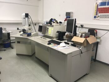
Absolute SEM
| Project Absolute SEM | |
|---|---|

| |
| Getting SEMsational images of chips, materials, and more! | |
| Status | In progress |
| Contact | User:Peterbjornx, User:Shiz, User:PeterC, User:noopwafel |
| Last Update | 2021-11-20 |
Background
After the pandemic brought the SEM_oud project to a standstill, and after the people running this project rented their own unit in the RevSpace building to have an office/lounge/arcade/misc space, it was decided to take our chances and buy a SEM without the level of scrutiny needed to restart the old project.
Status
After a quite adventurous trip to Germany (many thanks to User:eightdot for his help) we have succeeded in moving the SEM to Overgoo 1. Due to some unfortunate circumstances it is currently parked in RevSpace, but hopefully we will soon be able to move it out of there and start making it functional again.
Access
The SEM is located close to RevSpace and although it is privately owned, we will try to provide interested people with access once we get it working. What form this will take is still to be decided, but if anyone is interested feel free to talk to us once we get everything sorted.
Benefits
- We can image chips with ridiculous clarity
- We can image anything with ridiculous clarity, who needs normal microscopes
- It's a super cool device!
Use cases!
- Chip reverse engineering
- Chip failure analysis
- Metallurgy
- Detailed material analysis
- Biological analysis (subject to pre-processing depending on kind)
The SEM
- Model: Hitachi S-2300
- Precision: 4.5 nm
- Magnification: 20-200,000x
- Accelerating voltage: up to 30 kV
- Pump type: diffusion
- Built: early 90's
- Power required: 2kVA
- Digital image acquisition
- EDS (X-ray spectroscopy) detector: map out elements in sample