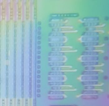
IC Reverse Engineering
| Project IC Reverse Engineering | |
|---|---|

| |
| Status | In progress |
| Contact | User:peterbjornx |
| Last Update | 2019-10-17 |
Introduction
Integrated circuits are a black box to most electronics hackers: the datasheet tells you how to interface to them and if you stick to this your project works. Sometimes, however, the chip does not behave as you expected it to, or the vendor decides to withhold information from you. In these cases you might want to take a look under the hood and see what makes the IC tick.
This project is about developing the tools and methods to do so. Some of these tools are taken from existing projects such as Decapping. Others are adapted from professional techniques, and others still are made up on the go.
Decapping
To start reverse engineering an IC, you first need to liberate the die (the silicon "chip"). The methods for doing this depend on the type of package.
Ceramic + sintered glass DIP packages
These are the packages used for EPROMs and 54-series glue logic. They consist of two ceramic slabs with the lead frame cemented in between them. You can easily open these with a pair of pliers by prying apart the slabs.
Ceramic lidded packages
These are used for processors and can be either DIP or PGA. They will either have one or two lids, and the lid is soldered in place using high temperature solder. Desoldering can easily be done using a torch.
Organic lidded packages
Mostly used by Intel for Pentium II and onwards. Taking the lid off by desoldering will not yield access to the die as the die void is filled with epoxy resin. This can be removed by trimming off the edges of the package and treating the die+epoxy part with molten colophony resin.