LichtKrant
| Project LichtKrant | |
|---|---|
| 350px | |
| Some 3-colour 80x7 pixel moving LED sign | |
| Status | In progress |
| Contact | bertrik |
| Last Update | 2019-12-16 |
Introduction
Found this moving LED sign on the revspace free stuff table.
It is 80 pixels wide, 7 pixels high. Each pixel has two sub-pixels (red and green), so it can display 3 colours (off, red, orange, green)
Goals:
- reverse engineer the electronics and document how it works
- replace the controller board with an ESP32, so we can receive image/text updates over the network
- implement more colour depth, so we can display gradient bitmaps (not just red, green, orange)
- write software for this, so other people can do the same for their display
Hardware

It consists of a processor board and a LED board.
Processor board
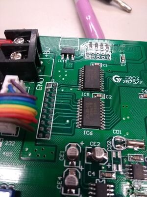
The processor board has a 8052, a flash chip, battery, 32768 Hz crystal, 40 MHz crystal, Altera Max chip. It appears the Altera chip drives two 245 chips which in turn drive the signal to the connector J1 to the LED board.
It takes 5V as input.
The PCB has a text on it: HXITC017_2.PCB
LED board
The LED board contains the actual pixels, organized in 16 modules of 5x7 LEDs. Each LED has a red sub-pixel and a green sub-pixel, so it can do colors: red, green, orange. The LED modules have the text GYXM-G2357ASRG on them.
The PCB has a text on it: HXBI80070509.PCN, date 2007-12-28
The are already electronics on it, consisting mostly of 595 chips (serial shift registers). The are two chains of 10 pieces of 74hc595 chips each, controlling the columns. There is an '138 chip (3-to-8 decoder) that drives a set of MOSFETS, 7 in total, controlling the rows. The MOSFETs are SDM4953, dual P-channel MOSFETs.
Reverse engineering the LED board electronics
This is done by tracing out the connections from connector J1, which connects the processor board to the LED board.
*  J1: pin IC5.A8 -> IC2.A1 -> IC2.B1 -> via ... -> shift clock
                  -> IC1.B1 -> IC1.A1 -> U11.SRCLK
                  -> IC1.B6 -> IC1.A6 -> U1.SRCLK
*  J2: GND?
*  J3: pin IC6.A1 -> IC2.A2 -> IC2.B2 -> via ... -> latch clock
*                    IC1.B2 -> IC1.A2 -> U11.RCLK
*                    IC1.B5 -> IC1.A5 -> U1.RCLK
*  J4: GND?
*  J5: pin IC6.A2 -> IC1.B3 -> IC1.A3 -> U11.SER -> data pin for upper shift register
*  J6: GND?
*  J7: pin IC6.A3 -> IC1.B4 -> IC1.A4 -> U1.SER -> data pin for lower shift register
*  J8: GND?
*  J9: pin IC6.A4 -> IC2.A7 -> IC2.B7 -> via ... -> row enable
                  -> IC4.1A -> IC4.1Y -> IC3.G2B
* J10: VCC?
* J11: pin IC6.A5 -> IC2.A3 (row) -> IC3.A -> row select
* J12: VCC?
* J13: pin IC6.A6 -> IC2.A4 (row) -> IC3.B -> row select
* J14: VCC?
* J15: pin IC6.A7 -> IC2.A5 (row) -> IC3.C -> row select
* J16: ???
* J17: pin IC6.A8 -> IC2.A6 -> IC2.B6 -> IC3.G2A -> row enable?
* J18: ???
* J19: ???
* J20: connected to the "ethernet" dipswitch

IC2.A7 <- IC4.1A <- via
          IC4.1A -> IC4.1Y -> IC3.G2B
- IC1 = 74HC245 (octal buffer) on LED board
- IC2 = 74HC245 (octal buffer) on LED board
- IC3 = 74HC138 (3-8 mux) on LED board
- IC4 = 74HC04 (hex inverter) on LED board
- IC5 = 74HC245 (octal buffer) on CPU board
- IC6 = 74HC245 (octal buffer) on CPU board
- U1-U10 = lower chain of 74HC595 (8-bit shift register)
- U11-U20 = upper chain of 74HC595 (8-bit shift register)
There are 8 rows (3 bits) controlled by the 74HC138 and 8 MOSFETS and two chains of 10x 74HC595 (8-bit shift registers) for the columns.
In summary, connector J1 has the following signals:
- rows
- 3-bits row select
- columns
- 1 bit shift clock shared for both shift registers
- 1 bit latch clock shared for both shift registers
- 1 data bit for 80-bit shift register 1
- 1 data bit for 80-bit shift register 2
- 2 row-enable bit signals, not completely figured out yet
- other
- 5V signals
- GND signals
- some signal for the infared remote control
Levels on the bus are 5V.
Software
The plan is to drive the display using an ESP32, with one core dedicated to the display and the other core for other tasks (e.g. receiving messages over the network).
Preliminary code can be found on the github lichtkrant repository.
Brightness is planned using a kind of duty-cycle modulation:
- For each pixel we keep a running brightness count (e.g. 8-bit).
- For each frame we add to it the brightness value from the frame buffer (e.g. 0-256). If the addition results in an overflow, the pixel is lit on the display. If no overflow occurs, the pixel is dimmed on the display.
- Each pixel on the display starts with a random count, so we avoid synchronised flashing of the pixels on the display. In other words, pixels with the same brightness have the same duty cycle, but have random turn-of/turn-off times with respect to each other.
Communication between the cores consists purely of the state of the frame buffer. The main core writes the frame buffer, the real-time display core reads the frame buffer and updates the LEDs.
Links
Possibly useful other info: