Absolute SEM: Difference between revisions
Peterbjornx (talk | contribs) |
Peterbjornx (talk | contribs) No edit summary |
||
| Line 60: | Line 60: | ||
* Biological analysis (subject to pre-processing depending on kind) | * Biological analysis (subject to pre-processing depending on kind) | ||
== Gallery == | |||
<gallery> | |||
Abs_sem_bug.jpg|Bug sputtered with gold | |||
Cracked_deschutes.jpg|Cracked CPU die | |||
Cracked_deschutes_closeup.png|Cracked CPU die (closeup) showing ~200nm vias and other structures | |||
</gallery> | |||
== Bibliography == | == Bibliography == | ||
Revision as of 17:59, 8 August 2022
| Project Absolute SEM | |
|---|---|

| |
| Getting SEMsational images of chips, materials, and more! | |
| Status | In progress |
| Contact | User:Peterbjornx, User:Shiz, User:PeterC, User:noopwafel |
| Last Update | 2022-08-08 |
Background
After the pandemic brought the SEM_oud project to a standstill, and after the people running this project rented their own unit in the RevSpace building to have an office/lounge/arcade/misc space, it was decided to take our chances and buy a SEM without the level of scrutiny needed to restart the old project.
Status
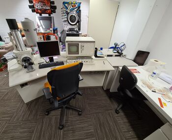
After a quite adventurous trip to Germany (many thanks to User:eightdot for his help) we have succeeded in moving the SEM to Overgoo 1.
It is now located in the Absolute Unit down the hallway from RevSpace.
We have had to repair several things:
- Remove rodent excrement from the SEM: full teardown of electronics and rebuild
- Replace the scintillator disk as it had degraded.
- Add shims under the vibration dampers as they had degraded leading to the column resting on the shipping posts
We are also working on adding some features such as a:
- Webcam chamberscope, with help of the Frees
- BSE detector (also with help of the mill, not done yet)
Access
The SEM is located close to RevSpace and although it is privately owned, we will try to provide interested people with access once we get it working. What form this will take is still to be decided, but if anyone is interested feel free to talk to us once we get everything sorted.
The SEM
- Model: Hitachi S-2300
- Precision: 4.5 nm (theoretical) 32 to 64 nm ( actually achieved so far )
- Magnification: 20-200,000x
- Accelerating voltage: up to 30 kV
- Pump type: diffusion
- Built: early 90's
- Power required: 2kVA (measured ~1500W)
- Digital image acquisition
- EDS (X-ray spectroscopy) detector: map out elements in sample
Benefits
- We can image chips with ridiculous clarity
- We can image anything with ridiculous clarity, who needs normal microscopes
- It's a super cool device!
Use cases!
- Chip reverse engineering
- Chip failure analysis
- Metallurgy
- Detailed material analysis
- Biological analysis (subject to pre-processing depending on kind)
Gallery
-
Bug sputtered with gold
-
Cracked CPU die
-
Cracked CPU die (closeup) showing ~200nm vias and other structures


