LichtKrant: Difference between revisions
| Line 75: | Line 75: | ||
There are 8 rows (3 bits). | There are 8 rows (3 bits). | ||
Two chains of 10x595 (each) for the columns | Two chains of 10x595 (each) for the columns, U11-U10 and U11-U20. | ||
In summary. | |||
* rows | |||
** 3-bits row select | |||
* columns | |||
** 1 bit shift clock shared for both shift registers | |||
** 1 bit shift register latch bit shared for both shift registers | |||
** 1 data bit for 80-bit shift register 1 | |||
** 1 data bit for 80-bit shift register 2 | |||
Levels on the bus are 5V (so can we drive it with an ESP?) | Levels on the bus are 5V (so can we drive it with an ESP?) | ||
Revision as of 23:10, 15 December 2019
| Project LichtKrant | |
|---|---|
| 350px | |
| Some 3-colour 80x7 pixel moving LED sign | |
| Status | Initializing |
| Contact | bertrik |
| Last Update | 2019-12-15 |
Introduction
Found this lichtkrant on the revspace free stuff table.
It is 80 pixels wide, 7 pixels high. Each pixel has two sub-pixels (red and green), so it should be possible to display at least 3 colours (red, orange, green)
Goals:
- investigate if we can drive this with an ESP8266
- investigate whether we can apply some kind of PWM to increase colour depth
- document how it works
- write software for this, so other people can do the same for their display
Hardware
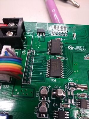
It consists of a processor board and a LED board.
Processor board
The processor board has a 8052, a flash chip, battery, 32768 Hz crystal, 40 MHz crystal, Altera Max chip. It appears the Altera chip drives two 245 chips which in turn drive the signal to the connector J1 to the LED board.
It takes 5V as input.
The PCB has a text on it: HXITC017_2.PCB
Connector pinout J1
*  J1: pin IC5.A8 -> IC2.A1 -> IC2.B1 -> via ...
                  -> IC1.B1 -> IC1.A1 -> U11.SRCLK
                  -> IC1.B6 -> IC1.A6 -> U1.SRCLK
*  J2: GND?
*  J3: pin IC6.A1 -> IC2.A2 -> IC2.B2 -> via ...
*                    IC1.B2 -> IC1.A2 -> U11.RCLK
*                    IC1.B5 -> IC1.A5 -> U1.RCLK
*  J4: GND?
*  J5: pin IC6.A2 -> IC1.B3 -> IC1.A3 -> U11.SER
*  J6: GND?
*  J7: pin IC6.A3 -> IC1.B4 -> IC1.A4 -> U1.SER
*  J8: GND?
*  J9: pin IC6.A4 -> IC2.A7 -> IC2.B7 -> via ...
                  -> IC4.1A -> IC4.1Y -> IC3.G2B
* J10: VCC?
* J11: pin IC6.A5 -> IC2.A3 (row) -> IC3.A
* J12: VCC?
* J13: pin IC6.A6 -> IC2.A4 (row) -> IC3.B
* J14: VCC?
* J15: pin IC6.A7 -> IC2.A5 (row) -> IC3.C
* J16: ???
* J17: pin IC6.A8 -> IC2.A6 -> IC2.B6 -> IC3.G2A
* J18: ???
* J19: ???
* J20: connected to the "ethernet" dipswitch

IC2.A7 <- IC4.1A <- via
          IC4.1A -> IC4.1Y -> IC3.G2B
- IC1 = 74HC245 (oct buf)
- IC2 = 74HC245 (oct buf)
- IC3 = 74HC138 (3-8 mux)
- IC4 = 74HC04 (hex inverter)
- IC5 = 74HC245 (oct buf) on CPU board
- IC6 = 74HC245 (oct buf) on CPU board
- U1 = lower chain of 595
- U11 = upper chain of 595
There are 8 rows (3 bits). Two chains of 10x595 (each) for the columns, U11-U10 and U11-U20.
In summary.
- rows
- 3-bits row select
- columns
- 1 bit shift clock shared for both shift registers
- 1 bit shift register latch bit shared for both shift registers
- 1 data bit for 80-bit shift register 1
- 1 data bit for 80-bit shift register 2
Levels on the bus are 5V (so can we drive it with an ESP?)
LED board
The LED board contains the actual pixels, organized in 16 modules of 5x7 LEDs. Each LED has a red sub-pixel and a green sub-pixel, so it can do colors: red, green, orang The LED modules have the text GYXM-G2357ASRG on them.
The PCB has a text on it: HXBI80070509.PCN, date 2007-12-28
The are already electronics on it, consisting mostly of 595 chips (serial shift registers).
There is an '138 chip (3-to-8 decoder) that drives a set of MOSFETS, 7 in total, so probably the row select.
The MOSFETs are SDM4953, dual P-channel MOSFETs.
Links
Possibly useful other info:
