Buiding up and testing the ZX81+38 revision 1,9
| Project Building up the ZX81+38 | |
|---|---|
| |
| A manual on how to build the ZX81+38 | |
| Status | Completed |
| Contact | mahjongg |
| Last Update | 2023-05-24 |
For those planning to build the ZX81+38, note this kit is NOT suitable for people who are not proficient in soldering. The ZX81+38 is not easy to solder, the design is dense and the solder pads are smaller than in most other designs. Also you will need to have the right tools, and probably a loupe or soldering microscope. You also need to own an EPROM programmer. I suggest using the minipro TL866CS to program a 27C256 with four copies of the ZX81.ROM file. and obviously you need experience like knowing resistor color codes etc etc, and owning a multimeter and know how to use it.
All files you need are on my GitHub page here: https://github.com/mahjongg2/ZX81plus38 as is a .PDF called building and testing a ZX81+38 I wrote from this experience.
Start Building with the lowest parts
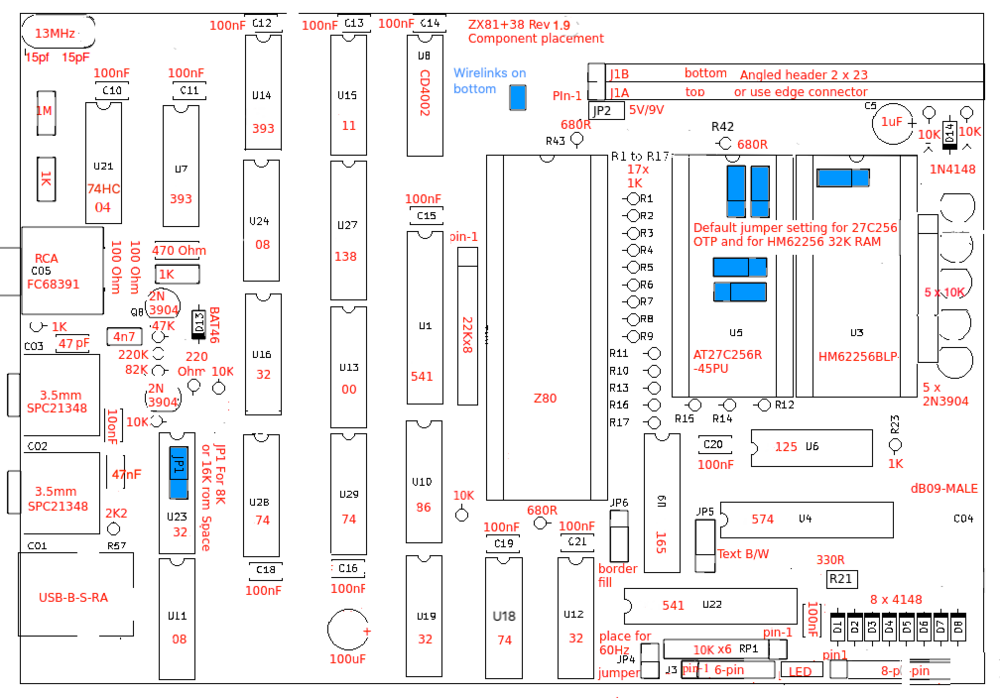
Make sure you use the latest files for the PCB, BOM and component overview drawing, and schematic, at this moment these are revision 1.9.
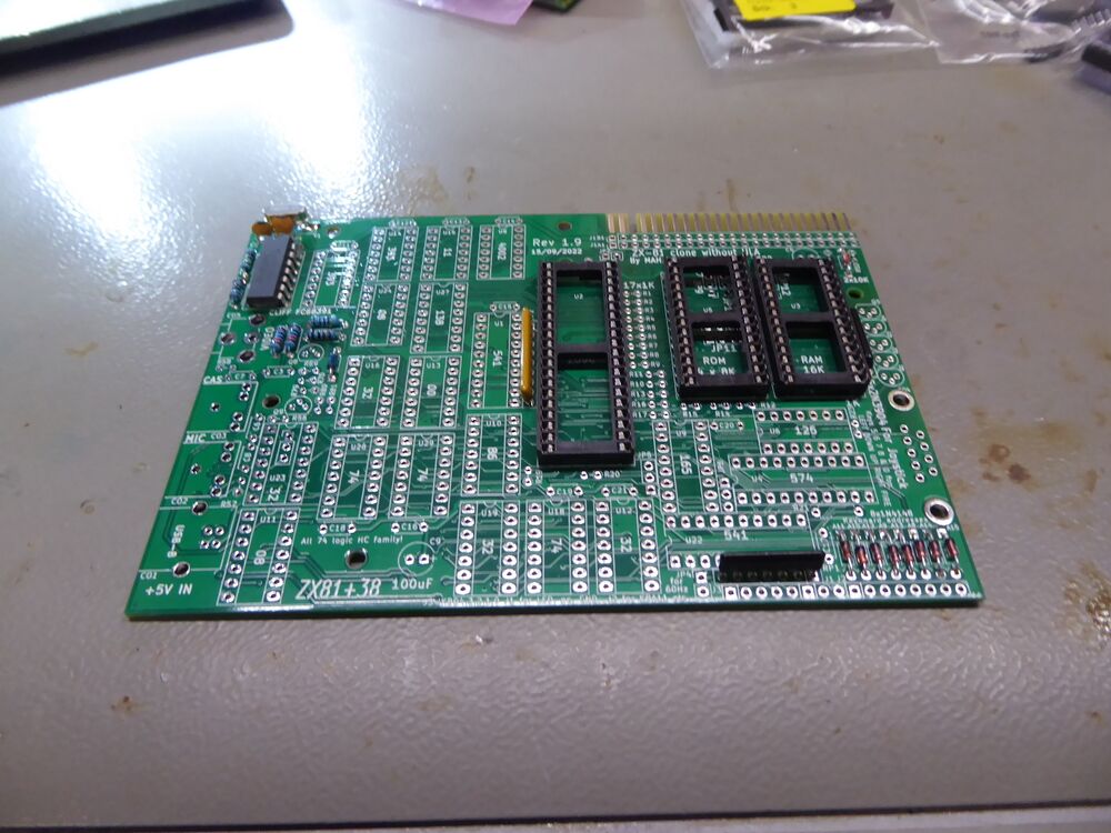
Start by soldering the lowest parts, that is, the flat lying resistors, and the resistor packs, and the diodes (the nine 1N4148 and the single BAT46 shottky diode), note their orientation! Also now is the time to place the three main sockets. see this picture:
Add the IC's
Then add the IC's be careful to place them in the right orientation, with their notches either up, or to the left, and in the right spot, referencing the component buildup drawing. Use the latest version of revision 1.9 of the component overview drawing, that is the drawing where the 15pF capacitors are BELOW the crystal. And use the latest BOM to order components, specifically make sure you buy the right connectors, as sometimes there a components that are just like them, but still different.
Note that I'm not using sockets for the other IC's, but you can if you want, if you do, use dual wipe sockets, NOT round machined sockets, as those are a disaster to put IC's into, and they are not as reliable as they seem to be. sockets that contact the IC pins from both the inside and outside are more reliable cheaper and easier to use.
If you see a number like "08" in the middele of in IC in the drawing this means you need the HC08 version of the IC, so "08" means you need to place a 74HC08 there. All logic IC's are HC type with A possible exception of the CD4002 which you can buy as 74HC4002 or as CD4002.
place the Crystal
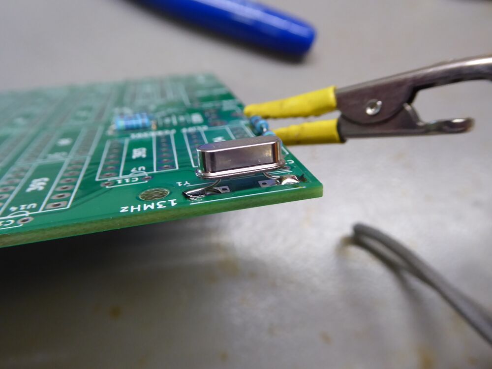
then place the 13MHz crystal If you could not find an SMT type of this crystal, the one that comes with a plastic carrier and flat pins sticking out besides the metal can, then convert your pin though hole crystal to a SMT solderable one by sticking the pin wires through a piece of paper, fold the pins flat sideways, and cut the wires off just outside the paper isolation.then solder the pins to the solder pads beneath. If you are carefull not to cause a short between the pins and metal can you might leave out the paper isolation, see:
next place the small ceramics
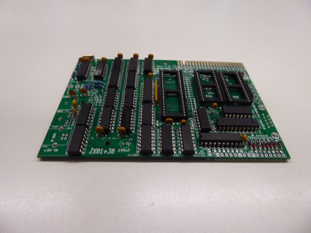
Now you can start with the small ceramic capacitors, use the component overview drawing and a highlighter marking which capacitor you have done. Start with all the special capacitors (all non 100nF decoupling caps) like the 15pF caps, and all the others, then add the 100nF decoupling caps. as in this picture:
And the two electrolytic capacitors and the standing up resistors
there are only two elco's in this design, a 100uF bulk capacitor, and a 1uF for reset, solder them in and notice their polarity. There are lots of upright resistors, especially the seventeen 1K resistors to the right of the Z80, but also others, note on the component drawing where they are which value they need to have and their orientation (chosen to make shorting two resistors together unlikely). use they highlighter to keep track of which you did. After sticking the wires through bent them out slightly so they won't fall out easily.
Add the connectors
After that you can start with the connectors, For the Cinch (RCA composite video out plug) I recommend the FC68391, do not use the reichelt CBP unless you have to, as its a very bad quality component. The fit is so tight that I had to wrangle the plug into it which promptly broke of the inner contact, I had to solder it back again. Not recommended, unfortunately Reichelt doesn't seem to sell any other suitable connector. Then solder the two 3.5mm audio jacks, tree models without in-built switches, make sure to buy the correct types with just three pins, there are other with completely different pinout, so be careful what you buy. lastly solder in the USB type-B (square) socket, I know its old and ugly, but it is the only suitable (USB) socket that is pin through hole.
And the transistors
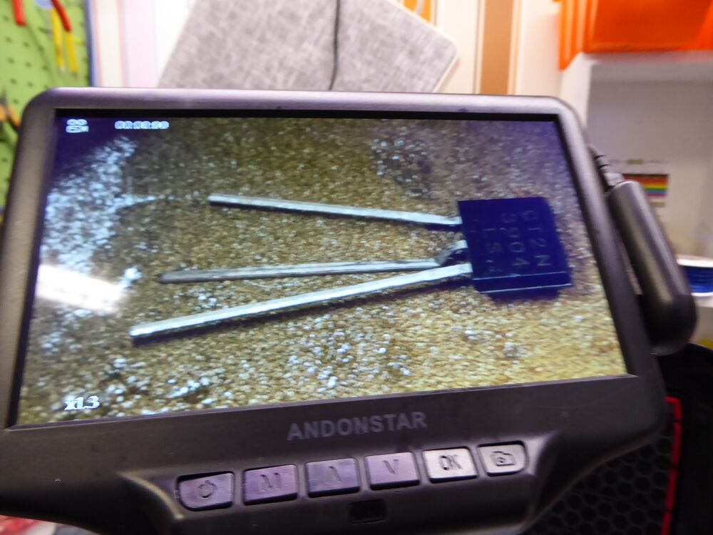
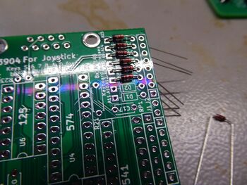
then you can add the seven 2N3904 transistors, if you bought the versions that have all three pins in a single line you might want to prepare the transistors, as otherwise it almost impossible to enter then in the PCB, so bent the middle pin towards the rounded part of the plastic, and then bent the wire up again a few mm (1/10 of an inch) so the pins are now in a triangle. The middle pin is now a few mm shorter than the other two, this helps inserting the pins, but it will be even easier when you also cut a few mm of rom one of the other two pins, ao all pins have different lengths, which makes interring them easy. like this:
Optionally add the joystick connector
If you want to add the joystick port you can add the male DE09 connector (often erroneously called a DB9 connector). But you may wait if you plan to use the original ZX81 enclosure, as you have to hack an opening in the case and you might not want to do this.
Now insert the Z80 CPU, the programmed ROM, and the 32K RAM chip, make sure the notch in the IC point to the back, same as shown in the component placement drawing. Note that ROM's especially don't like placing the in reverse! you will destroy them if you power up with them "upside down".
Attaching the keyboard
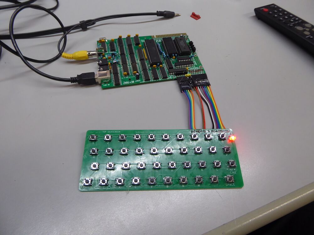
I'm using my own keyboard PCB, also on the GitHub page, with 40 6x6mm buttons (see keyboard BOM) I connected the keyboard to the PCB using dupont wires, with male sockets (that is those with pins) on the PCB side. On the PCB I used angled female headers, I simply took the kind of female headers as used on an arduino, cut of one pice with 5 pins, and another one with eight pins, and bent their pins 90 degrees. for the three pin segment in the middle I used a 3-pin male angled pinheader, and cut off the middle (unused) pin. for those two wires I used two female dupont wires. I cut the dupont wires all to the same length (about ten centimeters) stripped them twisted the wire strands together and tinned them. Stuck the wires though the keyboard PCB, and soldered them on top (it helps if you cut off the end bit of the tinned wire, and fold the wire flat to the top of the PCB, so the wire stays in place for soldering, but look out not to create shorts. after soldering the 5+2+8 wires use a small bit of hot glue on the underside of the board. If using the real ZX-81 top case with the keyboard foil removed, you might have to widen the slot underneath the keyboard so the wires can go though with key keyboard laying flat. But before you do test the zx81+38 without an enclosure. Like this:
If you see any errors or omissions in the above text please mail me at mahjongg@xs4all.nl.
test it!
If all is well and you have chosen composite video (or AV) in on your monitor, if you power the board on, the power led should light up immediately, and the screen will turn white, and after a a second or so the inverse K prompt will appear.
What to do If it doesn't work
In my case the result was just a black screen. :-(
A disappointment as I know the design works well, and I'm reasonably good in soldering, and triple checked all solder-joints, and re-soldered any and all suspect solder joints (it helps to hold the PCB to a light if you can see light shining through an un-soldered joint.
after the first day of debugging I already found several problems, but I still have a black screen, the ZX-81 is NOT an easy device to debug and this has bitten me! I didn't expect I had to debug this build, I had read many enthusiastic responses that it worked "first time". not for me though!
The first problem I found is that the RCA connector is a piece of sh*t. made out of scrap metal and recycled plastic I could have guessed it was no good, bit it still negatively surprised me how bad it really is. I once more suggest buying the must better version sold by farnell, but this was literally the only one sold by reichellt it is almost impossible to plug in the RCA plug, and as you try to wriggle it in (turning the plug while trying to push it in) you immediately break the metal that connects the PCB solder-point of the signal to the contact you are trying to plug into. So I saw the break in the metal, and the multi-meter confirmed there was a break in the connection. So I thought "that must be it", and soldered the broken connection.that worked, as the multi-meter proved. But my optimism was unfounded, I still had a black screen. so I did all the standard stuff, checking the voltages on the chips, all okay 4.98V then I checked reset it was high as it should. I tested the clock signal,with an oscilloscope and it ran. saw 3.25MHz on the CPU, so no problem there, but when I checked the databus signals all were steady low! en even stranger all the adress-lines were too! I removed the Z80 and saw it had one pin bent under it, but that wasn't it either. I checked if I forgot to tie nBUSRQ (pin 25 of the Z80) high, but R18 was present, not forgotten. I started to doubt the ROM, it was a W27C512 maybe one I didn't program. So I tried to use my TL866 II Plus programmer, and booted up windows 7, but the programming software refused to work claiming the program was old, it did start up and some things worked but not all. Removing the software din work, and installing a new version also didn't work, (I even had to install 7zip as winrar also refused to work) so I was stuck. I returned to my normal OS on my laptop, Linux mint, I did have the open source command line driven version of the TL866 programmer and it worked, (big win for open source IMHO) not as easy as the GUI version, but it worked. I dumped the ROM content, and that seemed okay, but comparing it with a concatenation of eight zx81.rom files said it was different. I now also began to doubt a W27C512 (not W27C256) would even work, so I cut the knot, and programmed a 27C256 I had bought with four copies of the ZX81.rom. that worked! The 27C256 programmed and verified fine, and a hexdump confirmed that it looked like four copies of ZX81.ROM were programmed into the 27C256 (256 / 8 = 32, so you need four copies of 8K 4 x 8 =32) , I used the linux cat command to concatenate the four copies into one larger file. I used:
cat zx81.rom zx81.rom zx81.rom zx81.rom > zx81x4.rom
I tried the 27C256 and I got a bit further, now there were data line signals and the address lines were active. Still no picture yet! To check if the ROM was running correctly I checked if the three bit column counter received its clock and reset signals, I could see U7B count from 0 to 7 on the ROW0 ROW1 and ROW2 signals. I also saw nSYNC pulses on U11b pin 6.
That were the first few hours, and I had to stop for the day...
when I was at home I wondered if it was necessary to place three pins pin-headers on JP5 and JP6 and put a correct jumper on them, but when I looked at the PCB I saw that the jumpers were already connected with a wire bride, so that the generated picture will be black letters on a white background, so that isn't the problem. Some people prefer white letters on a black background and in that case you need to cut the traces between the jumper pads, and jumper the tow jumpers in the other position. Not having any connections in JP5 and JP6 can indeed lead to no picture at all, but I added default jumping. so that cannot be it.
Day 2 debugging (I found it!)
I started with the one thing I really needed a schematic printout in A3 format. The schematic I had was too small to see the small texts without a magnifying glass. So with some trouble I printed the schematic on A3 format, and that actually helped a lot!
Well I did another test to see if the CPU ran the correct code, by testing if the CPU NOP enforcer U1 got nNOP pulses on pin 1, and it DID! so now I know for sure this is not a software (not running) problem!
I saw with the scope, that the VIDEO signal only outputted black pixels. So I followed the video output, and from the pixel shift register to the video out of U11A pin 3, and still I saw no problems, then I tried to measure the signal on 88, and when I put my scope probe on R49 suddenly the screen turned white! So I took the ZX-81+38 to the soldering station, and looked at R49 with the microscope, and I saw that the pin connected to +5V looked strange, I doubted it was soldered well, It looked like there was only solder paste around the pin, and yes, it wasn't making contact! So after I re-soldered it the ZX81+38 came to life, and I finally saw the cursor, the white 'K' in a black field!
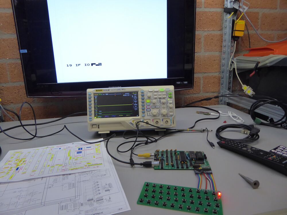
so I tried the standard canonical BASIC 10 PRINT "HELLO WORLD " and 20 GOTO 10, but neither the 0 or the P (print) key worked.
see this picture, where I tried which pins worked:
Day 3 fixing the keyboard
Last week I noticed when trying to type in the canonical BASIC test program
10 PRINT "hello world "; 20 goto 10
that the '0' and the 'p' key didn't work, but the '1' and '9' key did.
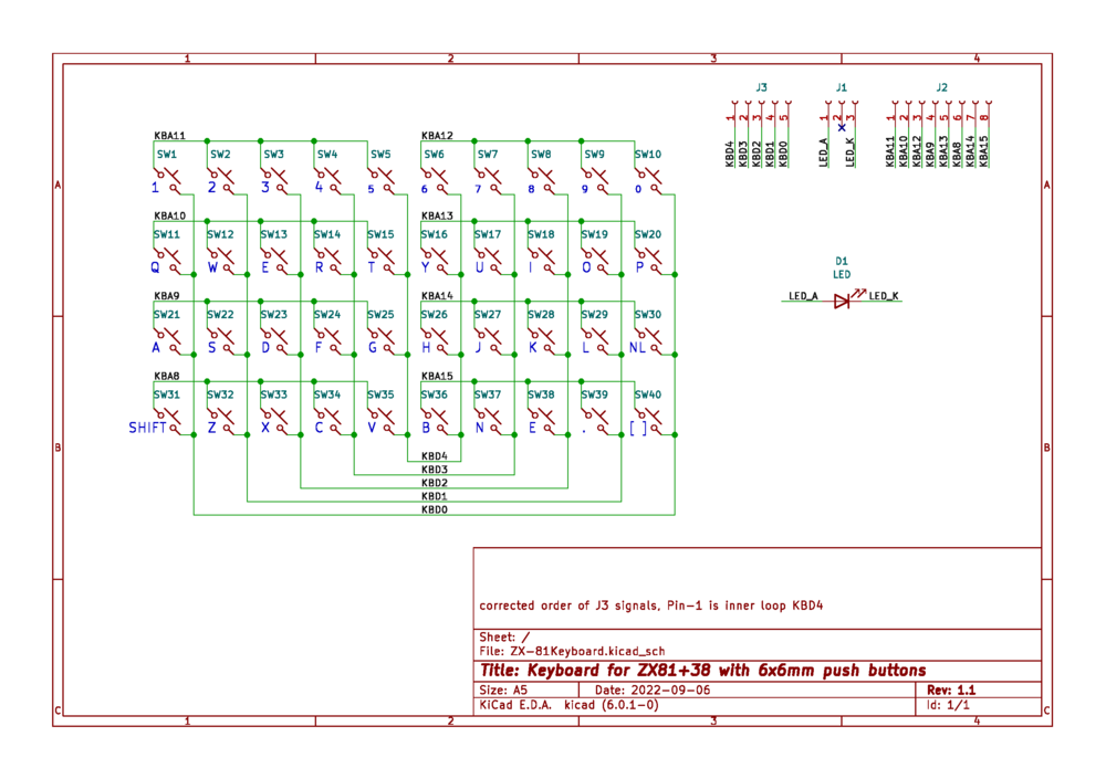
if you look at the keyboard schematic:
then you will notice that bot these keys use the same column (data) line KBD0, so I suspected an interruption in the cable connection for KBD0, but after visually inspecting and measuring the connection all KBDx and KBAx connections were fine, so that wasn't it. But as is the case with these 6x6mm buttons the keys itself are part of the routing of row and column lines, as the four pins are connected in two pairs, and I made use of this fact to layout the board on a single sided PCB, and so a single bad solder joint could break the matrix. The trick I used was to connect with a trace, these two pairs on the underside of the board, so I could use the connectivity check of KiCad, afterwards I simply did not use the bottom layer for the keyboard gerber file.
I inspected all four solder connections of all keys under our microscope, and I found a few where one of the four solder joints looked a bit dubious, and resoldered all dubious solder-joints, and after that all keys worked. I tested with the old military (teletype writer) sentence "the quick brown fox jumps over the lazy dogs back 1234567890" which includes all alpha and numeric keys, and they all worked fine.
So it seems the ZX81+38 is now fully operational, but perhaps I still need to test if loading and saving code works well but that is for another day.
I also need to test the Joystick port, but if I mount the DE09 male connector I have to cut a hole in the plastic of the original ZX-81 enclosure. So I first want to build the PCB into the case, and finish the keyboard with a new keyboard overlay, from plastified paper, without holes and simply glued to the corner keys, without cutting holes in the paper, and with the edges of the paper folded down. After that I will add the joystick connector, and test with a joystick (currently I don't own one, so that problem should be fixed first).
Finished, I wrote a build and test document
I used my experiences and photo's when writing this project file to write a .pdf explaining the process of building up a ZX81+38 and a small but essential testing guide, and uploaded it to my ZX81+38 GitHub area. with that I will mark this project as finished.
