Bestand:PTDC0012.JPG: verschil tussen versies
Uit RevSpace
GND and VCC wiring on bottom of PCB, right hand side of picture is left hand site when the PCB is turned with buttons up, with the "cross buttons". The lower two rows of pins will be soldered to the GPIO header, with two rows of two holes on either sid... |
Addig to category |
||
| Regel 1: | Regel 1: | ||
GND and VCC wiring on bottom of PCB, right hand side of picture is left hand site when the PCB is turned with buttons up, with the "cross buttons". The lower two rows of pins will be soldered to the GPIO header, with two rows of two holes on either side left over. | GND and VCC wiring on bottom of PCB, right hand side of picture is left hand site when the PCB is turned with buttons up, with the "cross buttons". The lower two rows of pins will be soldered to the GPIO header, with two rows of two holes on either side left over. [[Category:Pictures]] | ||
Huidige versie van 2 jul 2017 19:54
GND and VCC wiring on bottom of PCB, right hand side of picture is left hand site when the PCB is turned with buttons up, with the "cross buttons". The lower two rows of pins will be soldered to the GPIO header, with two rows of two holes on either side left over.
Bestandsgeschiedenis
Klik op een datum/tijd om het bestand te zien zoals het destijds was.
| Datum/tijd | Miniatuur | Afmetingen | Gebruiker | Opmerking | |
|---|---|---|---|---|---|
| huidige versie | 23 nov 2016 23:53 | 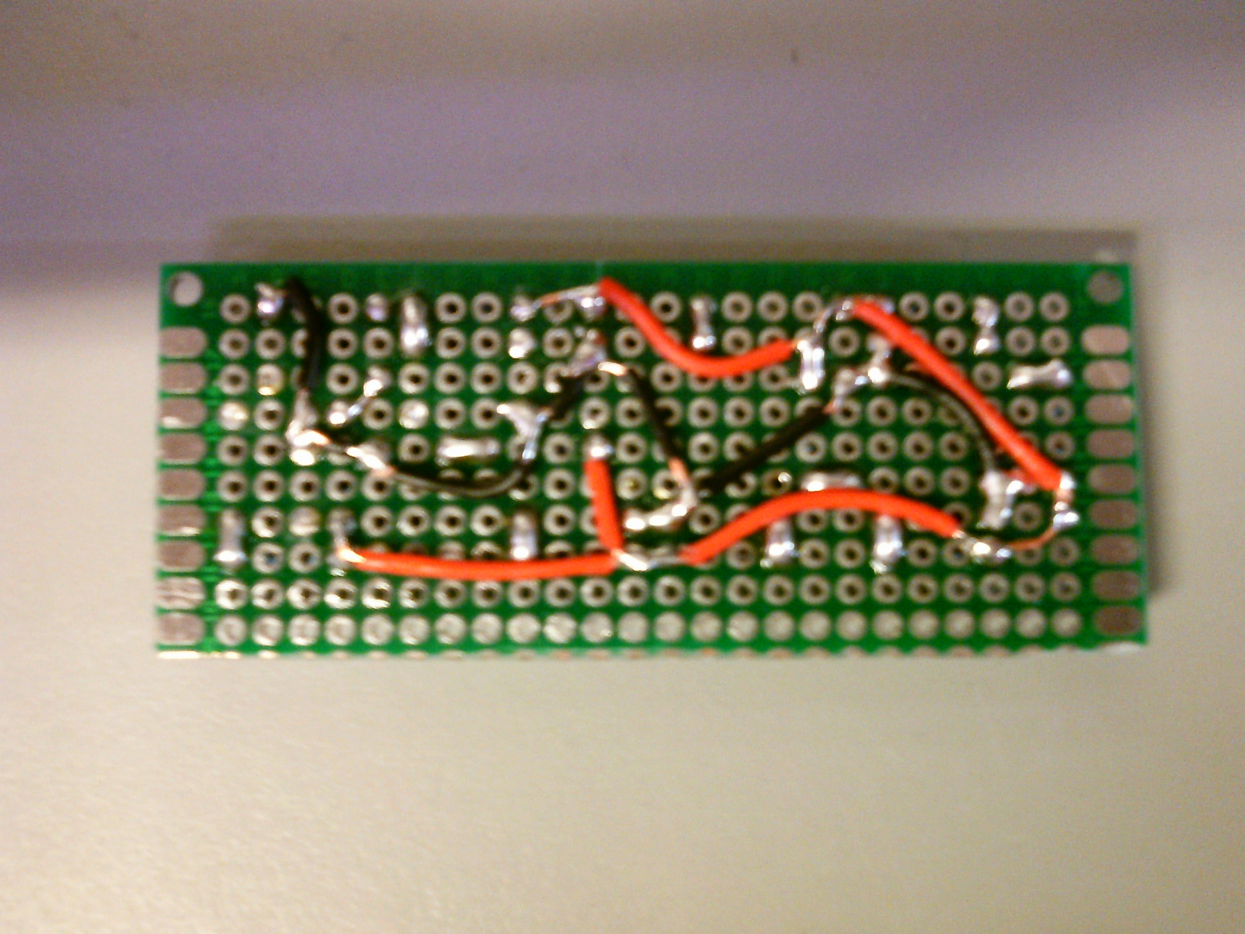 | 4.032 × 3.024 (1,86 MB) | Mahjongg (overleg | bijdragen) | GND and VCC wiring on bottom of PCB, right hand side of picture is left hand site when the PCB is turned with buttons up, with the "cross buttons". The lower two rows of pins will be soldered to the GPIO header, with two rows of two holes on either sid... |
U kunt dit bestand niet overschrijven.
Bestandsgebruik
Dit bestand wordt op de volgende pagina gebruikt: