Zon ZX-81 Programmable Sound Generator expansion for ZX81PLUS35 with working SD-Card: Difference between revisions
m (Dave o moved page Zon X-81 Programmable Sound Generator expansion for ZX81+35 to Zon X-81 Programmable Sound Generator expansion for ZX81PLUS35: replace + with PLUS) |
(add DISPLAYTITLE) |
||
| Line 1: | Line 1: | ||
{{DISPLAYTITLE:Zon X-81 Programmable Sound Generator expansion for ZX81+35}} | |||
{{Project | {{Project | ||
|Name=ZON X-81 PSG for ZX81+35 | |Name=ZON X-81 PSG for ZX81+35 | ||
Revision as of 17:30, 27 October 2016
| Project ZON X-81 PSG for ZX81+35 | |
|---|---|

| |
| Programmable sound generator for my ZX81 clone | |
| Status | In progress |
| Contact | Mahjongg |
| Last Update | 2016-10-27 |
The ZON X-81 is a sound generator based on the famous AY-3-8912 PSG.
This is a remake for my ZX-81+35 ZX81 clone. It features stereo sound outputs, and also enables the GPIO's, to which an SD-card slot is connected, which hopefully will enable, with help of some software expansion in ROM, to read SD-cards. Additionally the board serves (can serve) as an interface to a classical edge connector, or to another ZX81+35 expansion board (with pinheader connector).
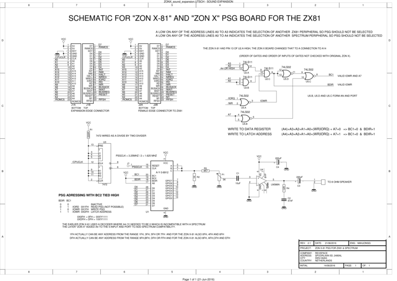
I started by investigating the original ZON X-81, and soon found out there were two verslons, the original ZON X-81 and the later, "Spectrum compatible" ZON X. For neither a schematic diagram seemed to be available, and there seemed to be some confusion about the I/O ports used. In the end I decided the best course of action seemed to be to use the available information to draw up my own schematic, and ask for input from the community. So I eventually came up with this. File:ZONX sound expansion REV 2,0.pdf
The ZON X (and presumably the ZON X-81 also) used just the minimum amount of logic to interface directly to the AY-3-8912 PSG, using just two 74LSxx logic IC,s a 74LS11 and a 74LS02 to access two 8-bit registers of the PSG, the data register and the index register. The data register is used to write data to one of the 18 registers of the chip, the index register is used to choose which one of the 18 registers is used. Some registers control GPIO ports of the chip, depending on the version of the chip there could be zero, one or two of these, the 8912 used has one eight bit port. But on the ZON X you can only write to any of the IO ports,due to the simple decoder logic used. it also used the ancient 7472 TTL chip to create a divide by two counter to divide the 3.25 MHz clock by two to a suitable 1.625MHz clock for the PSG. My guess as a reason for this even then strange choice was that the vendor of the ZON X-81, a company called BI-PAK that was know for selling cheap (3rd choice) transistors and IC's in packages called "BI-Pak" then, had quite some stock left over of 7472's, and decided to use them. in any case their interface logic worked, where many others had taken a look at the convoluted interface logic of the AY-3-8912 chips, and had decided against trying to directly interface to it (the AY-3-89xx series was designed to be interfaced with a CPU that lost the early "CPU wars", the ill faith-ed early PDP11 architecture based 16-bit general instrument CP1610, anyone remembers that one?, it used a completely different bus interface than thwo competing standards, the Motorola, and the Intel bus standard, so interfacing it to a Z80 which the "intel bus", was anything but simple. Most Z80 systems that used the AY-3-8912 therefore controlled it indirectly, often through a "PIO" chip like the intel 8255, as did for example MSX systems, and many others. BI-PAK decided against such an approach, and developed their interface from "fist principles", to be as cheap as possible. Much like the ZX81 itself.
My own (ZX81+35) version
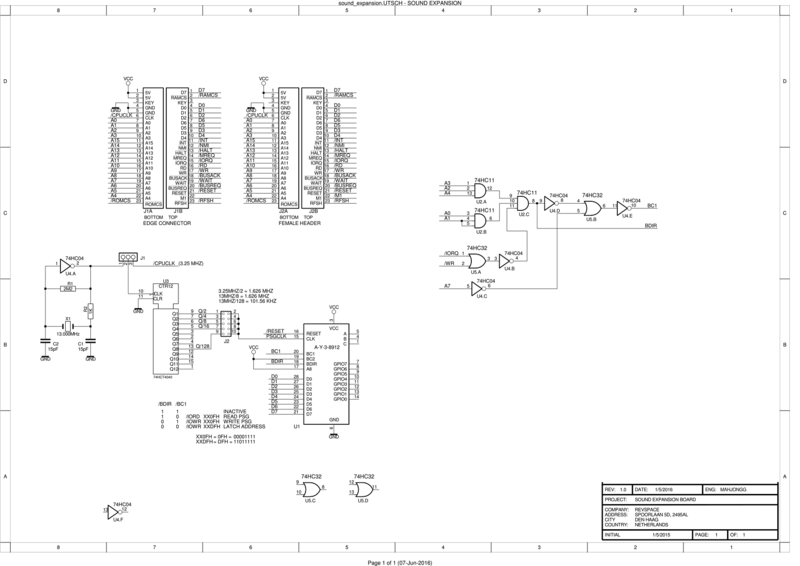
So, this was my initial starting point, and the revision 1.0 (unfinished) schematic was based on it, except for the audio output circuit, and a more flexible clock generator (at that point I still was not sure which clock frequency the ZON X-81 used, and I wanted an independent clock generator, as the clock of the ZX81+35 could also "randomly" double its clock signal to 6.5MHz (I consider changing that in the definitive version, so the output clock will always be 3.25 MHz even in turbo mode, so I don't need in internal clock generator in my PSG, it will also be more compatible with other expansions).
So this is the first beta revision schematic:
to do;
Remove extensive divider, and local xtal oscillator, add simple divider-by-two (1/2 74HC74). √ Done.
add audio output to stereo jack (mix A, B and C outputs) √ Done.
Add write register logic (Raise BC1 also during valid IORD cycle). √ Done.
add third port header for pinheader as in ZX81+35, as alternative for edge connector. √ Done.
add SD-card interface logic, need pullups on GPIO √ Done.
build prototype and test.
try to get to read (FAT32) SD-card using bit-bang driver.
first final version, without sd-card interface
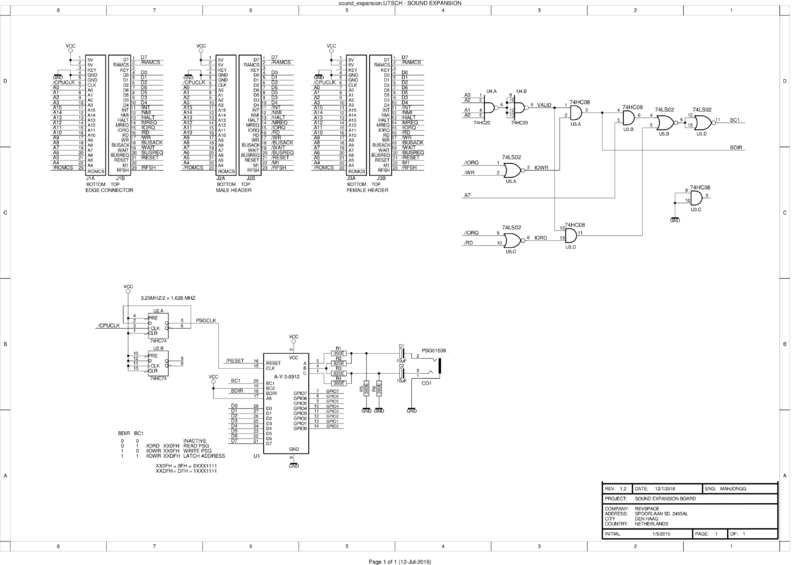
Revision 1.2, not using GPIOs: File:PSG for ZX81+35 REV 1.2.pdf
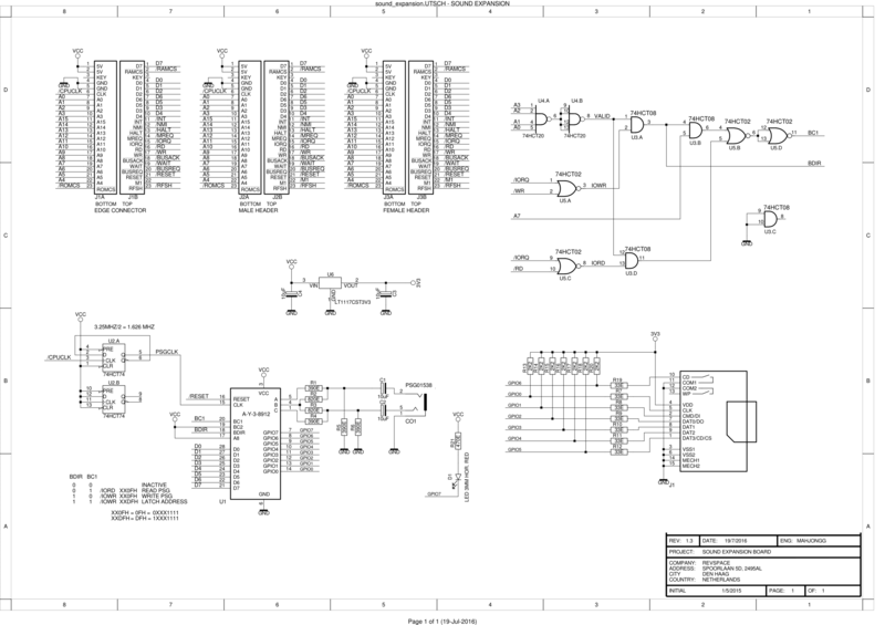
second final version, with sd-card interface
Revision 1.3: File:PSG for ZX81+35 REV 1.3.pdf
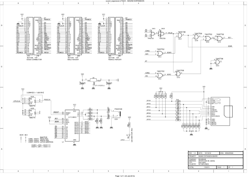
note, I made a mistake! the sd-card can output levels up-to 3v3, which is fine for the PSG (AY-3-8912), witch just needs a signal between 2.5V and 5V, but the PSG can output 5V levels (when the GPIO port is programmed as output) but the SD-card cannot cope with 5V levels. Initially I thought the PSG used open collector outputs, so I simply used pullups to 3V3, but I'm not sure the PSG won't output 5V levels, so the pullups to 3V3 serve no use (other than to keep the clock level stable high during use of a GPIO input) so the resistor setup should change so that a 5V output from the PSG reaches the SD-card as no more than 3V3 so I need to change the circuit so it uses a resistor divider. a pullup on the clock line is still needed to keep the clock line high during using the GPIO as input, to avoid spurious clock signals, but the pullup will be to 5V, not 3V3.
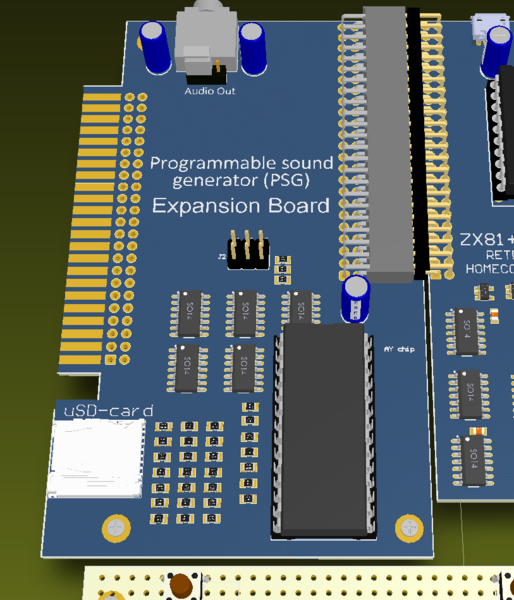
A preview of the board, created with Altium.
Revision 1.4 with level shifting resistor dividers
File:PSG for ZX81+35 REV 1.4.pdf
data lines are pulled up (both DO and DI are normally high) clock and latch (CS) are not as they are normally low, the lower part of the resistor divider act like pull downs so neither a clock or a trigger is generated during a GPIO read cycle (all GPIOs become either input or outputs together). The 22K resistors also split the bus to avoid damage should both the GPIOs and the SD-card try to put different data on the "bus". PS. I noticed that with the original resistor values the SD-card could not drive the PSG inputs low enough, so I updated the resistor values in the .PDF, the .PNG will be updated ASAP.
Revision 1.5 with multiple PSG board support
File:PSG for ZX81+35 REV 1.5.pdf
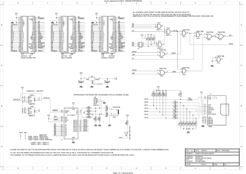
This version adds support for using two (or even three, if fan-out/fan-in and timing of the chips in the system allow it) PSG boards. It also adds support for using the PSG together with other boards that use A4, A5 or A6 as active low chip selects by adding three jumper locations with which you can disable the PSG for those "chip selects". When using two PSG boards you block one chip select for the primary, and another for the secondary board.
With two or more boards you can use a two wire (shielded) interconnect cable, so you can have six channel sound on one of the stereo jacks.
Revision 1.6, decided upon a DM3D Push-Pull micro-SD card reader
File:PSG for ZX81+35 REV 1.6.pdf
As said, I decided upon a cheap and cheerful, and easy to implement card slot, which schematic symbol is slightly different than the original, it does not have a write protect switch, and uses a different pin numbering.
this is the new picture:
september 2016
I had to put this project on hold, as I discovered that I rotated the edge connector 180 degrees on the ZX81+35, and decided that I needed to correct that before I could continue with the expansion card. It has taken me a few weeks, and will take a few weeks more to correct the ZX81+35 layout, it quite a big job. after that I will have to rotate the connectors in the expansion card too, to adjust to the new correct layout, with pin 1 at the bottom (towards the user). Actually the 3D preview already showed pin 1 like that (the square pad), but the actual layout was wrong. I'm quite determined the ZX81+35 should be 100% compatible, so there was simply no way I would keep this error in. Another problem in the ZX81+35 I still intend to solve is the behavior in turbo mode, I think I know how to fix it.
Revision 2.0 corrected rotation of expansion connector
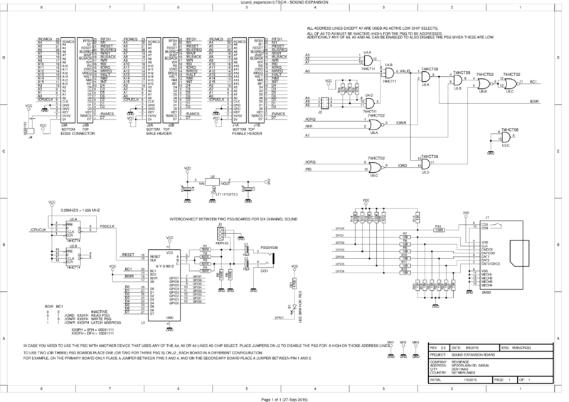
Resumed on PSG schematic on 27 September 2016. This version follows the correction of the rotation of the expansion connector, I did for the ZX81+35. File:PSG for ZX81+35 REV 2.0.pdf
Now continuing with the layout. Note the new ZX81+35 (Revision 4.0) now will always output 3.25MHz on the expansion connector, even in turbo mode. Also added jumper so its theoretically possible to put 9V DC on the edge connector pin that on an original ZX81 carries 9V DC, but on my clone has only 5V, this makes it possible to become compatible for those expansions that require the 9V DC by adding an extra external 9V supply.
