ZX81PLUS35 ZX81 clone: Difference between revisions
mNo edit summary |
|||
| (128 intermediate revisions by the same user not shown) | |||
| Line 4: | Line 4: | ||
|Picture=ZX81+35 revision 2.2 december 2015 front preview.png | |Picture=ZX81+35 revision 2.2 december 2015 front preview.png | ||
|Omschrijving=My clone of the Sinclair ZX81 | |Omschrijving=My clone of the Sinclair ZX81 | ||
|Status= | |Status= Completed | ||
|Contact=Mahjongg | |Contact=Mahjongg | ||
}} | }} | ||
My '''ZX81+35''', ZX-81 clone, previously called the ZX14 ZX15, and ZX81+34 (2015 Version) retro homecomputer is a much improved Sinclair ZX81 [http://oldcomputers.net/zx81.html] clone built with the modern materials techniques and components of 2015. | |||
The ZX81+35 will be built and tested in 2016. | The ZX81+35 will be first built and tested in 2016. | ||
Afterwards I got many comments that for a kit it was too difficult to build due to the use of SMT, which is a "bridge too far" for many hobbyists. | |||
So I also started on a much simpler to build ZX81+38, which can be mounted in an original ZX81 case, and is more a real clone, just with re-created ULA logic with discrete (PTH) logic chips. This is now (june 2020) finished. and berbers are uploaded to GitHub. | |||
it will be fully open sourced effort (but note that the original design of the ZX81 and its BASIC interpreter firmware is still owned by Amstrad) | '''The ZX81+38 is now the preferred version, and is designed to be used as a drop-in replacement of the PCB of a real ZX81, with conventional DIP IC's replacing the ULA.''' | ||
Note that due to the corona crisis (and the fact that I'm currently unemployed, so low of disposable cash) I have not yet build and tested the later ZX81+38 version, but as its based on the same schematic, I'm 99.9% sure it will work file. | |||
more info about the new ZX81+38 here: [https://revspace.nl/ZX81plus38_simple_to_build_ZX-81_clone] | |||
Some history about why I wanted to create a ZX81 clone can be found here: [https://revspace.nl/index.php?title=Zx81plus34] | |||
it will be fully open sourced effort (but note that the original design of the ZX81 and its BASIC interpreter firmware is still owned by Amstrad, although they have announced that using it is fine, you can find ZX81 ROM images online) | |||
As for now comments and questions on the design can be made here [http://www.raspberrypi.org/forums/viewtopic.php?f=62&t=77429&p=551927#p551927] (raspberry PI forum off topic section) :-) | As for now comments and questions on the design can be made here [http://www.raspberrypi.org/forums/viewtopic.php?f=62&t=77429&p=551927#p551927] (raspberry PI forum off topic section) :-) | ||
| Line 39: | Line 49: | ||
# No need for the original ULA, it is replicated with conventional logic. | # No need for the original ULA, it is replicated with conventional logic. | ||
# Cheap to build by using low cost components, on small dual sided PCB, with single sided assembly only. | # Cheap to build by using low cost components, on small dual sided PCB, with single sided assembly only. | ||
# Design files | # Design files are freely available on GitHub from july 31 2019 (but do note that firmware is still © Amstrad!) | ||
== Inspirational sources used for the design of the ZX81+35 == | |||
ZX81 rebuild projects I investigated to get inspiration from: | |||
* wilf rigter's "THE ZX97LITE SCHEMATIC DISASSEMBLED Rev.pdf" | |||
* wilf rigters "turbo.pdf" | |||
* wilf rigters "ZX81WAIt.pdf" | |||
* Kevin bakers, "turbo switch circuit.gif" redrawn by wilf rigter | |||
* Rodney knaaps ZX81 rebuilds # 1, #2 and #3 | |||
* "ZX81 ULA Replacement By Andrew Rea.pdf" | |||
* "zx96mainboard schematic.gif" | |||
* Alwin Henseler's "ZX81_ULA-in-a-CPLD_v1.10.zip" | |||
* grant searle's "ZX80nmiVer4.1.jpg" slow mode extension for ZX80 | |||
* PokeMon's "ZX80CORE-manual-EN.pdf" | |||
* Andy Rea "mini ZX81" page 1 to 4 | |||
* Other ZX80 /ZX81 info: | |||
* "ZX81 Service and Assembly Manual (scans) kopie.pdf" | |||
* "The Complete zx81 Rom Disassembly.pdf" | |||
* "Assembly Listing of the Operating System of the Sinclair ZX80..html" | |||
* "zx80_schema redrawn A3.pdf" | |||
* "Sinclair ZX80/81 etc Specifications.pdf" | |||
* "graphic view of zx81 rom.jpg" | |||
* "ZX81 schematic highres.jpg" | |||
* "Microace_Diagram_s1.jpg" | |||
* "annotated redrawn zx80-schema.gif" by NoCash | |||
* "brazilian slow mode adapter schematic .jpg" part 1 and 2 | |||
* "ZX81CCP_schematic.jpg" | |||
* "jupiter ace 4000.pdf" by Bodo Wenzel | |||
* "cp-200 (ZX81 clone) schemas" | |||
* "tk82 (ZX81 clone) schemas" | |||
* "power 3000 (lambda 8300) schematic.gif" | |||
* "ts1500 schematic (scan).gif" | |||
== Status, from January to march 2015 == | == Status, from January to march 2015 == | ||
| Line 64: | Line 105: | ||
== Schematic 81+34 == | == Schematic 81+34 == | ||
The old (version 1) schematic of revision 2.0 (.PDF) can be found here: [[File:ZX81plus34 schema.pdf]] | The old (version 1) schematic of revision 2.0 (.PDF) can be found here: [[File:ZX81plus34 rev2.00 schema.pdf]] | ||
There is also a color coded schematic (.PDF), it can be found here: [[File:ZX81plus34 kleur | There is also a color coded schematic (.PDF), it can be found here: [[File:ZX81plus34 kleur rev 1.0.pdf]]. | ||
Note that SMT components are depicted purple, and PTH ones green. | Note that SMT components are depicted purple, and PTH ones green. | ||
| Line 88: | Line 129: | ||
Here is the schematic (plus board layout) of the keyboard: | Here is the schematic (plus board layout) of the keyboard: | ||
[[File:KB matrix schematic.pdf]] | [[File:KB matrix schematic.pdf]] | ||
Note this schematic is the corrected version that is compatible with a real ZX81, so it uses the address order A11, A10, A12, A9, A13, A8, A14, A15 | |||
It doesn't include connections for LED's or the reset input. | |||
I also designed a new keyboard overlay suitable for such a keyboard with the keys going through holes in the overlay. | I also designed a new keyboard overlay suitable for such a keyboard with the keys going through holes in the overlay. | ||
| Line 337: | Line 380: | ||
* Changed T8 to a faster PMEG2005 transistor for better picture quality | * Changed T8 to a faster PMEG2005 transistor for better picture quality | ||
here is the updated .PDF, further updates are likely: [[File:ZX81plus35 REV 3.0.pdf]] | here is the updated .PDF, further updates are likely: [[File:ZX81plus35 REV 3.0 13 3 16.pdf]] | ||
== March 15, 2016 fixed the video problem == | == March 15, 2016 fixed the video problem == | ||
| Line 349: | Line 392: | ||
== March 23 2016 first attempt to get cassette port working == | == March 23 2016 first attempt to get cassette port working == | ||
Unfortunately there were, and are several problems with the cassette port, output and input. Both on the input and output I reversed left and right channels. My intention was to only use the left channel, (TIP) and ignore the right channel (RING) but unfortunately the pin I used in both cases was for the right channel. I fixed that problem. The next problem was the transistor pre-amp, it reversed the input signal, normally no big deal as the audio signal can be reversed without a problem. Still the ZX81 software expects the signal to be low, with high going pulses, but due to the transistor the signal the software saw was high with low going pulses. After several failed attempts to find a simple solution, and doing some measurements on the kind of levels coming out of my laptop I decided there was plenty enough signal and no amplification was necessary. So I removed the transistor from the design. | Unfortunately there were, and are, several problems with the cassette port, output and input. Both on the input and output I reversed left and right channels. My intention was to only use the left channel, (TIP) and ignore the right channel (RING) but unfortunately the pin I used in both cases was for the right channel. I fixed that problem. The next problem was the transistor pre-amp, it reversed the input signal, normally no big deal as the audio signal can be reversed without a problem. Still the ZX81 software expects the signal to be low, with high going pulses, but due to the transistor the signal the software saw was high with low going pulses. After several failed attempts to find a simple solution, and doing some measurements on the kind of levels coming out of my laptop I decided there was plenty enough signal and no amplification was necessary. So I removed the transistor from the design. | ||
Because I used CMOS logic I deemed it necessary to add protection diodes against negative signals, and signals larger than 5V. Unfortunately I have not been able to save and load any program yet, so this is just a temporary fix. Even though my new design is not fully patched, and what I have did not work, I still updated the schematic, and uploaded it here. | Because I used CMOS logic I deemed it necessary to add protection diodes against negative signals, and signals larger than 5V. Unfortunately I have not been able to save and load any program yet, so this is just a temporary fix. Even though my new design is not fully patched, and what I have did not work, I still updated the schematic, and uploaded it here. | ||
| Line 359: | Line 402: | ||
== March 27 2016 designed a reasonably well working cassette input port == | == March 27 2016 designed a reasonably well working cassette input port == | ||
Well I gave given this much thought. I found inspiration in the Timex/Sinclair official ZX81 extended clone the TS1500. It had an improved cassette interface, and yes, it was using a transistor, but just slightly different than my first transistorized attempt. | Well I gave given this much thought. I found inspiration in the Timex/Sinclair official ZX81 extended clone the TS1500. It had an improved cassette interface, and yes, it was using a transistor, but just slightly different than my first transistorized attempt. | ||
There were some doubts about the values used, so I plugged the schematic into LTSpice, the Analog design simulator of Linear Technology, which is free to download and use. | There were some doubts about the values used, so I plugged the schematic into LTSpice, the Analog design simulator of Linear Technology, which is free to download and use. and this is what I came up with after intensive value tweaking: | ||
[[File:Picture of Spice model of cassette interface ZX81+35.png|700px]] | [[File:Picture of Spice model of cassette interface ZX81+35.png|700px]] | ||
| Line 412: | Line 455: | ||
I will also try running some variations of high-resolution software to see just how compatible my ZX81 clone is. | I will also try running some variations of high-resolution software to see just how compatible my ZX81 clone is. | ||
== 1/4/2016 ( = 4^0 / 4^1 / 4^2 ) Updated preview == | == 1/4/2016 ( = 4^0 / 4^1 / 4^2 ) Updated 3D preview == | ||
In preparation of the design for (the 3D rendering of) an enclosure I updated the preview ( done with | In preparation of the design for (the 3D rendering of) an enclosure I updated the preview ( done with Altiums 3D rendering ). The corrections are a better proportion of the PCB, (previous previews did not have the exact 10 x 10cm dimension of the real boards, (but more 9.2mm high by 10mm wide), the current preview corrects that. The preview now also uses realistic male/female angled pinheaders for the interconnect between keyboard and PCB, (so the outer dimensions of the enclosure are now known) the size of the expansion board was adjusted so it uses the available space more effectively, and planned mounting holes were added to mount PCB, expansion board and keyboard to the bottom halve of the planned enclosure. I will get my inspiration from the QL. | ||
the updated preview replaces the previous rev 2.0 preview, and page header and project thumbnail pictures. | the updated preview replaces the previous rev 2.0 preview, and page header and project thumbnail pictures. | ||
in time I will design 3D rendering of the two "clam shell" halves so you can get an impression of how the ZX81+35 would look in its enclosure. | in time I will design 3D rendering of the two "clam shell" halves so you can get an impression of how the ZX81+35 would look in its enclosure. | ||
| Line 448: | Line 491: | ||
== On april 12, 2016 I was diagnosed with Sleep Apnea, which means I cannot drive a car! == | == On april 12, 2016 I was diagnosed with Sleep Apnea, which means I cannot drive a car! == | ||
This means I will have | This means I will have very limited access to RevSpace :-( | ||
The good new is that I now know that I have Sleep Apnea (Apneu in Dutch) which means that I have over 30 breathing stops in my sleep each night, which nearly wake me up. Its the reason for being tired all the time, and for my subconscious fear of going to bed which has lead to a very strange biorhythm. | The good new is that I now know that I have Sleep Apnea (Apneu in Dutch) which means that I have over 30 breathing stops per hour in my sleep each night, which nearly wake me up. Its the reason for being tired all the time, and for my subconscious fear of going to bed which has lead to a very strange biorhythm. | ||
Also good news is that apnea is treatable, with an overpressure (APAP) device I will need to wear in my sleep, I will get a test for one next week (normally it takes over a week, so I'm lucky). Id did a sleepover at MCH and can say the APAP device worked very well for me, I will be offered one in two to three weeks time, I can't wait! If I used it for 2 months and it works well, I will get my permission to drive back. | Also good news is that apnea is treatable, with an overpressure (APAP) device I will need to wear in my sleep, I will get a test for one next week (normally it takes over a week, so I'm lucky). Id did a sleepover at MCH and can say the APAP device worked very well for me, I will be offered one in two to three weeks time, I can't wait! If I used it for 2 months and it works well, I will get my permission to drive back. | ||
| Line 477: | Line 520: | ||
== Found basic, but major error in ZX81+35 Updating to rev 4.0 == | == Found basic, but major error in ZX81+35 Updating to rev 4.0 == | ||
While designing the PSG expansion board I look once again to the expansion port and made a discovery that made me say some expletives &*$$$#)**^& ! I've made a mistake in the very beginning about the orientation of the expansion connector, such that it is now upside-down to how it should have been. This error is expressed in how the expansion connector was drawn in the schematics, (which probably explains the origin of the error) with pin 1 on top, and pin 23 on the bottom, but the edge connector should have been just rotated 90 degrees clockwise, which means pin 1 should have been on the bottom, not on the top! | While designing the PSG expansion board I look once again to the expansion port and made a discovery that made me say some expletives &*$$$#)**^& ! I've made a mistake in the very beginning about the orientation of the expansion connector, such that it is now upside-down to how it should have been. This error is expressed in how the expansion connector was drawn in the schematics, (which probably explains the origin of the error) with pin 1 on top, and pin 23 on the bottom, but the edge connector should have been just rotated 90 degrees clockwise, which means pin 1 should have been on the bottom, not on the top, that is, If I wanted to be compatible with a real ZX81, which I do!! | ||
This means a very large layout modification is necessary to accomplish this. I could have "fixed" it by rotating the pins on the PSG board, but in my opinion that is cheating. Its a genuine error and has to be fixed! | This means a very large layout modification is necessary to accomplish this. I could have "fixed" it by rotating the pins on the PSG board, but in my opinion that is cheating. Its a genuine error and has to be fixed! | ||
| Line 511: | Line 554: | ||
doing that to URL's pointing to .PNG pictures might be trickier as changing the URL may delete the picture itself in this thread, until the pictures URL is also changed. | doing that to URL's pointing to .PNG pictures might be trickier as changing the URL may delete the picture itself in this thread, until the pictures URL is also changed. | ||
So for now I only replaced URL's not used in pictures. until i'm informed the pictures are copied to ones using "plus" instead of "+" in their filename. | So for now I only replaced URL's not used in pictures. until i'm informed the pictures are copied to ones using "plus" instead of "+" in their filename. | ||
There was also the case of another page like this, (https://revspace.nl/ | There was also the case of another page like this, (https://revspace.nl/Zx81plus34) a predecessor of this page talking about why I wanted to create the ZX81 clone that could not be accessed because it also had a "+" in the file name, but I managed to copy it to a new version with plus in the file name instead of + without help from the web master, its here [https://revspace.nl/Zx81plus34] | ||
== 29 November 2016, website problem mostly solved == | |||
I managed to find replacements for all the .PDF's and a few .ODF (BOM's) in this thread, and uploaded them with filenames without using the + sign | |||
There will be a few pictures on this page that when clicked upon will give a redirect error, but I hope that won't be a problem. | |||
== 2017 has arrived == | |||
Its now 2017, and Revspace has just moved to a new location, and I feel my ZX81+35clone is almost finished, but not yet completely. | |||
Thought about updating the name to ZX81+36, but rejected it (for now). | |||
There is one last Issue I would like to solve, and that is to get turbo working, without the screen shake that it has now. | |||
I fear that the problem is in the mechanism that switches the clock from turbo to normal when a screen has to be drawn, it seems the moment between the horizontal sync pulse and when characters are started to be clocked out is affected by when the mechanism decides to run in turbo mode, and when not. The solution it seems is to switch turbo off during the whole period of generating the screen, and only turn it on during the vertical sync period. I still have to decide how to do that, it will take some experimenting. I hope to finish the ZX81+35 after my intermittent projects have finished. Hopefully I will also be able to test my PSG board with it before I release the design, but testing it is made more difficult with my old (second) prototype because the expansion header has rotated 180 degrees. | |||
I also have to make a prototype board of the PSG to do that. | |||
== Its 2019 and I have decided to release my ZX81+35 == | |||
Even through I never got turbo mode (clock speed doubling) to fully working, as a ZX81 clone ZX81+35 works more than fine, and there seems to be some interest in it, so I released it under a BSD-3 licence (free to use and copy for non commercial use). | |||
You can find all the files you need to build your own version on GitHub here: https://github.com/mahjongg2/ZX81plus35 | |||
it now includes: | |||
* Schematic for revision 4.0 (the latest version) as a .PDF ([[File:ZX81plus35 REV 4.0.pdf]]) | |||
* Bill of materials (updated to the latest version) as .ODS (spreadsheet) | |||
* Ulticap and ultiboard files of the schematic and layout (CAD files) | |||
* production files (gerbera and drill files for revision 4.0) you can upload to any PCB manufacturer to get your own PCB (only main PCB, for now, not keyboard PCB, but you can hand build one with perfboard) | |||
* previews of the Top and bottom of the revision 4.0 PCB, so you can see what the PCB should look like. | |||
* keyboard overlay as .PDF (original version) you can plasticise it, and stick it over your keyboard. | |||
to come (I'm working on it): | |||
* Keyboard PCB layout | |||
I have also released prototype schematics and layout of my ZON compatible expansion board for a programmable sound chip on another GitHub page named "PSG-for-ZX81plus35-ZX81-clone". | |||
this expansion board adds AY-#-8912 sound generation, and a SD-Card slot through the PSG's expansion ports. | |||
This PSG board should be compatible with software for the ZON board for the ZX81, such as the dancing demon program, and some others, and can be used to create "chiptunes". | |||
It also serves as an expansion interface so you can use ZX81 peripherals that use an edge connector (the board brings out a real ZX81 edge connector), and can be used as an example how to add peripherals to my ZX81 clone. Note that I never had the chance to test it with older versions of my ZX81+35, as it needs the corrected expansion bus, (that only revision 4.0 has) and I never built the revision 4 version. | |||
So this expansion board has not been tested by me, but I believe it is correct, feedback if you do test it is appreciated (use the thread in the off-topic section of the raspberry PI foundation, or e-mail me at mahjongg at xs4all.nl | |||
== August 22, 2019 Started on the Keyboard PCB, compatible with the keyboard overlay == | |||
Although I designed the schematic (using UltiCap) and build a working prototype on Perfboard, I never did finish a real PCB for it. | |||
I will design one using KiCad, no way I'm going back to my old windows laptop, and try to use UltiCap and UltiBoard again. | |||
I want to retire that laptop forever. | |||
So here is the schematic for a Keyboard PCB compatible with the ZX-81+35, meaning that the order of the data and address wires is correct, and other pinheader positions are correct. For example the three pins for LED's are in-between the data and address headers. In this case the 18-wires are in the order nRESET, RESET-GND, KD4, KD3, KD2, KD1, KD0, POWER-LED, TURBO-LED, LED-GND, KA11, KA10, KA12, KA9, KA13, KA8, KA14 and KA15. | |||
The keyboard PCB can be connected to the ZX81+35 through a piece of 20-way flat flex cable with wire ends (https://nl.farnell.com/te-connectivity/fst-22a-20/ribbon-cable-ptfe-20way-2/dp/1310356), with 2 wires removed, soldered to the keyboard PCB on one end, and stuck into an 18-pole female socket on the main PCB. | |||
The schematic of the keyboard has been thoroughly researched so that I'm sure it will be compatible with both my clone, and with a real ZX-81. | |||
There seem to be some differences in the order of keyboard connections between a ZX-81, and a Spectrum, which confuses things. | |||
it seems that compared to the ZX-81 Spectrum keyboard wiring has KA9 and KA12 swapped. | |||
Note that in the ZX-81 the PCB seems mounted upside down, but this is actually an optical illusion because the PCB is mounted to the TOP case half, not the bottom half, so keyboard and PCB have the exact same orientation, just like my own design). | |||
I will do extra checks to make sure my wiring order is correct, for that I have arranged a real ZX-81 (plus memotech memory extension) to do extra compatibility checks, and check some dimensions, such as the keyboard recess, which I could not find online. | |||
My prototype keyboard had roughly the same size as the original, although a tiny bit larger, but now I have designed the keyboard PCB so that its outer dimensions are such that it exactly fits inside the recess of a real ZX-81, (after you round off the PCB corners a bit with a file) and its flat wire connection should fit exactly through the slit in the real ZX-81 enclosure. This means the PCB is 2.5 inch high, and 6.2 inch wide, this is a preview of the placement, of the buttons, and connectors, and the PCB size. | |||
[[File:ZX-81 Keyboard-F.SilkS.pdf]] | |||
Its probable that the buttons in this layout will move a bit up, to make place for 5 wires of Data wiring underneath. the full PCB has not yet been routed, but I foresee this will be necessary. | |||
The reset can be a simple push button mounted on the side (or back) of the enclosure. | |||
The carefully checked keyboard schematic for the ZX81plus35 is here: | |||
[[File:ZX-81plus35 Keyboard.pdf]] | |||
and this is a picture of this .PDF: | |||
[[File:ZX-81plus35 Keyboard PCB schematic.png|900px]] | |||
The keyboard uses forty 6 x 6 mm buttons ( MCDTS6-2N or equivalent ) with a 6.5 mm x 4.5mm pad pitch (long ends connected) with about 0.9mm thick pins (hole size of PCB = 1.1mm). These are very common. Make sure you use keys with a reasonable long stem, so they stick out well above the keyboard template. The stem width should be about 3.5mm, and the stem should be round. | |||
For connection to a real ZX-81 you can use a piece of FST-22A-15 flat flex cable with wire ends, (https://nl.farnell.com/te-connectivity/fst-22a-15/ribbon-cable-ptfe-15way-2/dp/1310375 ) cut into 5 wire and 8 wire parts, soldered to the underside of the PCB. The PCB can then be mounted to the plastic case. After removing the old foil keyboard, and sticking the FST-22A cable ends through the opening in the case, the PCB can then be screwed to the case with four 2.5mm self tapping plastic screws, after drilling four small 1.5mm holes in the case. the other ends of the flat-flex cables should fit into the sockets on the zx-81 main board. | |||
If you don't want to use the expensive FST-22A cable, its also possible to solder wire ends to cheap standard flat-flex foil cables, (https://nl.farnell.com/c/cable-wire-cable-assemblies/cable-assemblies/ffc-fpc-flat-flex-jumper-cables?searchref=searchlookahead) and solder the wire ends to the keyboard. If you first stick the flex-foils into the connectors, so their orientation is such that they make contact with the connectors, one being 180 degrees rotated relative to the other. | |||
== September 2, 2019 Made a new component overview (assembly drawing) for rev 4.0 == | |||
[[File:ZX81plus35 silkscreen overview rev4.png]] | |||
== September 11, 2019 Keyboard ZX81+35 PCB finished == | |||
Will save the files to GitHub, but here is a preview: | |||
[[File:Keyboard PCB ZX81plus35.png]] | |||
I managed to design it on a single sided PCB, using the fact that pairs pins of the switch over the long size are connected together, so can be used as wire bridges. | |||
This is how the component-side of the PCB will look, note there is no solder mask (green lacquer) layer, but it does have a white silkscreen (text print). | |||
[[File:ZX81+35 keyboard top.png|1000px]] | |||
and this is the solder side (mirrored) with soldermask. | |||
[[File:ZX81+35 keyboard bottom.png|1000px]] | |||
== I'm considering designing a simplified (to build) version, based on an ULA replicate == | |||
The current ZX81+35 design is nice, but has a few deficits that make it difficult to build, as a kit. | |||
I'm considering to simplify the build, by designing a ULA replacement, based on an FPGA with my ULA replacement logic in it, and also to build a replica ZX-81 clone for it which has only (a small amount of) PTH components on it, very similar to the original ZX-81 kit. | |||
It will be a more classical design, looking more like a real ZX-81 in size and shape, not restricted to a 10x10cm PCB, with (expansion) connectors in roughly the original locations, no need to worry too much about the infamous "wobble problem" with 32K of RAM (LY62256) on board, so returning to an edge connector in the back, and also with an 8K Byte FLASH ROM in a DIP package as PCB space is no longer a premium. | |||
The main job this time will be to replicate the original ULA, I'm planning to create one that will also work in a real ZX-81, so it will be a small QPF on a 40-pin carrier board, this will be a separate project. | |||
This time it will be done in KICad. | |||
watch this space. | |||
p.s. This idea never happened instead I simplified the plus35 by creating the plus38, which only uses pin through hole (PTH) technology, and leaves out all the stuff not necessary for a ZX-81 clone, and uses a PCB that is size and drill hole compatible with a real ZX-81. | |||
== If you have build a ZX81+35 and have a problem, you can reach me here == | |||
I have gotten reports about a person who has built my ZX81+35, and needed help solving a (minor) problem, and I realised I have given no address where you can reach me if you have a problem building my clone. | |||
You can reach me at ,mahjongg commercial-at xs4all.nl, (no need to publish my full e-mail address for mail address scanners to find). | |||
obviously I will be happy to give you free advice on how to find a problem, and might also offer free repairs, within reason (for example I Won't "repair" a ZX81+35 that has been powered with 12V) LOL. | |||
Someone attended me that the component overview drawing contains an error. U13 is listed as a 74HC32, while in fact its a 74HC00. | |||
Also there is a problem with downloading the BOM spreadsheet. Both problems are now fixed. | |||
== October 21, 2016 Received a free built ZX81+35 and its working == | |||
I only had to build an adapter for my keyboard, as I still wanted to keep it working for my own Revision 2.0 copy, but revision 2 uses the old wiring scheme. | |||
[[File:ZX81+35 revision 4.0 with keyboard.JPG|800px]] | |||
This is a program I tested it with: | |||
10 FOR X = 0 TO 255 | |||
20 PRINT CHR$ X; | |||
30 NEXT X | |||
and this is the resulting output, it is simply perfect, all characters fit perfectly together, and are clean and sharp: | |||
[[File:Printing all 256 characters.JPG|800px]] | |||
I found one small error while testing board, a text printed on the PCB near the turbo switch was wrong! sliding the switch to the left sets it in turbo mode, and to right in normal mode, but the text on the PCB claims that left is normal mode, and right is turbo mode. I would suggest disabling turbo mode, by wiring the switch position permanently to the right. Meantime a new silk screen file was created and updated in the GitHub production files .ZIP. The component overview drawing has also been corrected, and now shows default jmper positions. | |||
in turbo mode the display becomes unstable and jumps from left to right during printing. | |||
I could do a new attempt to find the cause. | |||
I can also try a patch to generate loading bars during a cassette load. | |||
== June 2020 I received news about errors in the latest gerber files == | |||
There seems to be slipped in a wrong file among the gerber files I uploaded in October 2020, it seems the top solder mask layer was a wrong one, and did not belong in the .ZIP file I uploaded to Github. | |||
when I downloaded the gerber files myself I could see there was something wrong, especially in the top right hand corner. | |||
These picture shows screenshots of the gerber files I downloaded from GitHub end June, 2020, left the full picture right details showing errors in the soldermasking. | |||
a.o. Missing pads for C26 and R70 so this is the old rev 4,0 version, '''don't use this to create PCB's!''' | |||
[[File:Old Gerbers Rev 4,0.png|500px]] [[File:Old gerbers Rev 4,0 detail.png]] | |||
Because of the corona lockdown, which also affected RevSpace, It took me some time to investigate the problem, also because I needed an old, and previously written off laptop, that has no battery and a French keyboard, but it has the now defunct CAD software with which I designed the ZX81+35. | |||
For the new ZX-81+38 I bought a new Laptop, and switched to KiCAD, and I hoped I would never have to use the old beast again. | |||
But I decided the only way to solve the problem reliably was to get the old laptop back and get it to work again, and create a completely new set of corrected gerber and drill files revision 4,1 | |||
So these are pictures of the gerber viewer showing rev 4,1 | |||
[[File:New Gerbers Rev 4,1.png|500px]] [[File:New Gerbers Rev 4,1 detail.png|500px]] | |||
I visually checked if these gerber files are identical to the known good previous build of the revision 4.0 of august 2019, which I know is working well | |||
I have uploaded the Gerber files, and also a Rev 4,1 Schematic (for completeness as its identical to the rev 4.0 one) to GitHub | |||
If you want the latest schematic, here it is: [[File:ZX81+35 REV 4.1 schematic.pdf]] | |||
== May 16, 2022 Yes after the two year long corona crisis has happened I'm back == | |||
I have good news, I just found out that an anonymous german ZX-81 enthusiast, I will call Thomas, has built this ZX-81 clone, but not only that, but he also built the PSG. | |||
He got everything working, including getting sound with the dancing demo "game", but not only that! He thought he could get the SD-Card interface working, an idea I gave up on because I could find no way to de-select the SD-Card (the chip-select /CS signal going to the SD card) while switching from a read to a write mode and back. If I tried to do that the SD-card would be de-selected, and so driving the SD-card seemed impossible, and I gave up on this idea, but Thomas not only found a way to circumvent the problem, he actually got the SD-Card interface working with minor patches, so he designed and implemented the patches, but also wrote the firmware to drive SD-Card reading, and wrote an menu driven user interface! To make using the card easy he stored his code in a 8K ROM expansion, so he patched the ZX81+35 so it would support 16K ROM. | |||
Because an SD-Card interface that only works when you load firmware from tape is not worth much! | |||
Actually the sd-card is at least ten times faster than loading from tape, and is much more convenient as you have a menu to choose a game from. see more here:https://revspace.nl/Zon_ZX-81_Programmable_Sound_Generator_expansion_for_ZX81PLUS35#15_march_2022.2C_great_news_a_PSG_board_builder_has_gotten_the_SD-card_interface_working and here (Im planning a version for real ZX-81's and my other clone the zx81+38 https://revspace.nl/Zon_ZX-81_compatible_PSG_%2B_32K_RAM_and_SD-Card_interface_expansion_for_ZX-81_and_clones | |||
Well this is such a great development that I have decided to make it official, so I will design new versions of the ZX81+35 (for extra 8K ROM support) and a new version of the PSG board, with his patches. | |||
keep watching here, and the PSG project page, for updates... | |||
== May 21, 2022 revision 4.2 supports 16K ROM space, and corrects some errors == | |||
I Updated the schematic and layout with revision 4.2, which now will support a (default) ROM space of 16K instead of the previous 8K, so you can put 16 K of code into the flash ROM chip, instead of the previous 8K, The new 8K extension can be used to place the firmware for SD-Card support in, so you can run the SD-card menu system without having to load anything from tape when using my programmable sound card AY-3-8912 ZON-ZX81 PSG card with a SD-Card reader built in. | |||
Also I repaired a hardware bug, Address lines A13 and A14 were erroneously swapped in revision 4.1, that is now corrected, also changed (although I would not call it a correction) is that now the expansion port uses the same clock signal "0" as the CPU, that is it will now chance clock speed with turbo mode turned on, but note that turbo mode is still not working correctly with video generation, its advised not to use turbo mode anyway, unless you only use FAST mode. | |||
The new schematic (In colour) is here: | |||
[[File:ZX81+35 REV 4.2. schematic color.pdf]] | |||
I also finished the new Layout, here is a preview of it: | |||
[[File:ZX81+35 REV 4.2 layout preview.PDF]] | |||
You can use the older placement diagrams as (except for the 8K/16K ROM patch resistors below U23) the component placement has not changed. | |||
see: https://revspace.nl/File:ZX81plus35_silkscreen_overview_rev4.png | |||
I will upload Gerber and drill PCB production files on my MAHJONGG2 GitHub pages soon: | |||
Latest revision as of 18:18, 5 April 2022
| Project ZX81+35 ZX81 clone | |
|---|---|

| |
| My clone of the Sinclair ZX81 | |
| Status | Completed |
| Contact | Mahjongg |
| Last Update | 2022-04-05 |
My ZX81+35, ZX-81 clone, previously called the ZX14 ZX15, and ZX81+34 (2015 Version) retro homecomputer is a much improved Sinclair ZX81 [1] clone built with the modern materials techniques and components of 2015. The ZX81+35 will be first built and tested in 2016.
Afterwards I got many comments that for a kit it was too difficult to build due to the use of SMT, which is a "bridge too far" for many hobbyists. So I also started on a much simpler to build ZX81+38, which can be mounted in an original ZX81 case, and is more a real clone, just with re-created ULA logic with discrete (PTH) logic chips. This is now (june 2020) finished. and berbers are uploaded to GitHub.
The ZX81+38 is now the preferred version, and is designed to be used as a drop-in replacement of the PCB of a real ZX81, with conventional DIP IC's replacing the ULA. Note that due to the corona crisis (and the fact that I'm currently unemployed, so low of disposable cash) I have not yet build and tested the later ZX81+38 version, but as its based on the same schematic, I'm 99.9% sure it will work file.
more info about the new ZX81+38 here: [2]
Some history about why I wanted to create a ZX81 clone can be found here: [3]
it will be fully open sourced effort (but note that the original design of the ZX81 and its BASIC interpreter firmware is still owned by Amstrad, although they have announced that using it is fine, you can find ZX81 ROM images online)
As for now comments and questions on the design can be made here [4] (raspberry PI forum off topic section) :-)
Introduction to the ZX81+35
The ZX81+35 is a much improved ZX81 that people can build themselves.
The ZX81+35 should be fully compatible with the original ZX81, but with the following improvements over the original ZX81 :
- Includes turbo option switch giving more than double (220%) the speed of the original, with turbo LED, and dynamic turbo slide switch.
- Includes 16KB of RAM instead of the original 1K (should also support 32K mode) but should be compatible with "high resolution" software.
- RAM can be made permanent with a battery backup system (optional) so program remains even during power off
- Supports ZX81 BASIC in either a EEPROM or in an OTP (one time programmable ROM) P.S. version 2 uses FLASH with a total of 16 8K banks.
- Compatible with modern TV's thanks to better digital sync signal generation, giving sharp stable and high contrast pictures.
- Composite video (PAL or NTSC) output signal instead of RF signal, for even sharper picture, compatible with yellow RCA inputs, and SCART
- Wobble free real expansion connector (can be modified to be fully compatible with the ZX81) modules can fit inside ZX15 enclosure, compatible with ZX81 printer
- Uses simple microUSB chargers as power supply, with low power consumption
- Can drive a simple 2x16 LCD display, and some external I/O for "stand alone" applications like driving tiny robots. Debug LED/Backlight LED support.
- Simple sound generation (full sound only when using fast mode)
- Supports a DB-9 joystick with up-down-left-right and fire, immediately compatible with games that use keyboard arrow keys (5,6,7 and 8) and 0 for "fire"
- Supports keyboard with real (moving) keys, using new keyboard overlay with holes for the keys, uses cheap 6x6mm buttons, keyboard layout also available. Using the original keyboard is also possible
- More sensitive and reliable cassette tape interface (can be reliably driven by MP3 players and such)
- Includes reset button option, and power LED.
- Alternative (nicer) ZX81+34 font available, to replace the standard one in the ROM.
- No need for the original ULA, it is replicated with conventional logic.
- Cheap to build by using low cost components, on small dual sided PCB, with single sided assembly only.
- Design files are freely available on GitHub from july 31 2019 (but do note that firmware is still © Amstrad!)
Inspirational sources used for the design of the ZX81+35
ZX81 rebuild projects I investigated to get inspiration from:
- wilf rigter's "THE ZX97LITE SCHEMATIC DISASSEMBLED Rev.pdf"
- wilf rigters "turbo.pdf"
- wilf rigters "ZX81WAIt.pdf"
- Kevin bakers, "turbo switch circuit.gif" redrawn by wilf rigter
- Rodney knaaps ZX81 rebuilds # 1, #2 and #3
- "ZX81 ULA Replacement By Andrew Rea.pdf"
- "zx96mainboard schematic.gif"
- Alwin Henseler's "ZX81_ULA-in-a-CPLD_v1.10.zip"
- grant searle's "ZX80nmiVer4.1.jpg" slow mode extension for ZX80
- PokeMon's "ZX80CORE-manual-EN.pdf"
- Andy Rea "mini ZX81" page 1 to 4
- Other ZX80 /ZX81 info:
- "ZX81 Service and Assembly Manual (scans) kopie.pdf"
- "The Complete zx81 Rom Disassembly.pdf"
- "Assembly Listing of the Operating System of the Sinclair ZX80..html"
- "zx80_schema redrawn A3.pdf"
- "Sinclair ZX80/81 etc Specifications.pdf"
- "graphic view of zx81 rom.jpg"
- "ZX81 schematic highres.jpg"
- "Microace_Diagram_s1.jpg"
- "annotated redrawn zx80-schema.gif" by NoCash
- "brazilian slow mode adapter schematic .jpg" part 1 and 2
- "ZX81CCP_schematic.jpg"
- "jupiter ace 4000.pdf" by Bodo Wenzel
- "cp-200 (ZX81 clone) schemas"
- "tk82 (ZX81 clone) schemas"
- "power 3000 (lambda 8300) schematic.gif"
- "ts1500 schematic (scan).gif"
Status, from January to march 2015
At the moment the PCB of the first prototype (ZX81+34) has been designed, and is ready to be tested.
26/01/2015 2 PCB's are being made, waiting for delivery next week, also a component order list has been created. 27/01/2015 A component placement diagram has been made, and has been published here. 31/03/2015 one PCB has been assembled, a keyboard is being made, (the first keys I bought were unsuitable due to too short plungers so I bought new ones. A programmed EEPROM needs to be made, I will probably design my own EEPROM programmer. Problem is that I used a 32K classical EEPROM, which has a different pinout than 64K and bigger sizes, for which FLASH versions are available. This means I must use a real EEPROM programmer, instead of being able to flash program the PROM. Ill design a raspberry PI based simple programmer, also useable for other replacement of other RETRO EEPROMS.
25/09/2015 could not get the first model to work (found faults in the schematic, but main problem is that many of the logic circuits were damaged when I applied the 5V with reversed polarity due to a wrong microUSB definition). Started on revision two, with all the bug fixes and acquired knowledge.
3D Preview of early ZX81+34
Before I even designed the PCB I made a mockup with Altium. Here are two (3D rendered) previews of the ZX81+34 board, to the top one is an older small preview of the complete system, including how I envisioned the whole system with keyboard would look like, at the bottom you can see a picture of the more recent 3D rendering of ZX81+34 PCB, and to the right, as a size reference the original ZX81. Note both PCB's are about equally as tall (10 cm), but the ZX81+34 is much smaller, as it square, while the ZX81 is much wider than it is tall.

The botom picture also shows, on the right, the four chips of the original ZX81, and on the left, what replaces them on the ZX81+34, green is the Z80 CPU, RED the (EE)PROM, Yellow the RAM (1K on the ZX81, 16/32K on the ZX81+34). Blue indicates the logic of the ULA, contained in a single 40-Pin IC on a ZX81, the ZX81+34 replicates it with 24 conventional but modern logic ICs.

Schematic 81+34
The old (version 1) schematic of revision 2.0 (.PDF) can be found here: File:ZX81plus34 rev2.00 schema.pdf
There is also a color coded schematic (.PDF), it can be found here: File:ZX81plus34 kleur rev 1.0.pdf.
Note that SMT components are depicted purple, and PTH ones green.
The Bill of Material (BOM) for the original ZX81+34 can be found here File:Z81plus34 BOM.ods

Layout ZX81+34
Even though I was hospitalized, then immobilized for several months (in the months of June July and August 2014) due to an operation on my leg, I still managed to work a bit on the layout of the ZX14. And on November 25, 2014 The layout work reached 100% connectivity. Here is a preview of how the work was progressed at that time . Clean-up, optimizing and copper filling followed somewhat later. The picture below on the left was actually a screen shot from a gerber viewer of how the board looked in September 16, 2014, note the lack of copper fill to make it easier to follow the connections around. Some weeks later the cleanup was ready, and this is a picture of how the PCB will more or less look like, when it is finished.


Keyboard for ZX81+34/35
Early on I was also busy designing a solution for the keyboard. My solution was to use commercially available cheap 6x6mm buttons, which (with some effort by bending the pins a bit) can be mounted on an EuroCard sized piece of 1/10"raster perfboard, the result would like something like the picture on the left.
Here is the schematic (plus board layout) of the keyboard: File:KB matrix schematic.pdf Note this schematic is the corrected version that is compatible with a real ZX81, so it uses the address order A11, A10, A12, A9, A13, A8, A14, A15 It doesn't include connections for LED's or the reset input.
I also designed a new keyboard overlay suitable for such a keyboard with the keys going through holes in the overlay. On the right is a drawing showing how it would look, note the brown dots are actually the actuators of the push buttons going through the holes in the overlay.
Here is a .PDF version that should be correctly scaled when printed on A4 paper. You can also use it to create a replacement keyboard for your ZX81.
A version that supports the ZXPand can be downloaded here: File:New ZX81plus34 keyboard ZXPand version.pdf


Alternative font for ZX81+34/35
I also designed an alternative (fun) font for the zx81+34 that can replace the one in ROM, it should be compatible with existing software, so graphic symbols are unchanged. As inverted characters are a hardware function, inverted characters (and graphics) are simply inverted copies of the original characters. Here is a preview.

Here is the original ZX81 character set to compare it with.

I know that big changes were not possible, but note for example the 4 and the A X and Y, and the addition of serifs to many characters.
The final ZX81+34
Finally mid January 2015 the PCB of the ZX81+34 was finished, a grounded mounting hole was added (needed to mount in an enclosure, to shielding). The picture below is a 3D rendered preview, some of the texts on the preview are there to comment some of the functions, and will not be present on the silkscreen of the final PCB.

The assembly drawing of the ZX81+34
Here is a drawing to help assembling the right components at the right places (A placement drawing), it was made from the real silkscreen gerber-file (in red) comments and component values in black.
Note that the values of R39 to R40 are wrong, they should be 22K not 1K!

Starting the assembly

just started with soldering the various resistors with a hot air soldering station
Finished assembly

Assembly of the ZX81+34 and its keyboard has finished. Still waiting for a programmed EEPROM before it can be tested.
The bare board looks like this:

Design of a (wooden) enclosure has started, also there is a chance I can lend an EEPROM programmer.
Testing (continued)
After I finally managed to program an EEPROM, I started testing the device, unfortunately disaster struck immediately! I could not get the device powered up, and after some searching I found out I made a mistake in the creation of the footprint of the microUSB connector, that caused the reversal of the GND and 5V pins. This means that for some time (minutes) the whole device was fed with negative 5V, a disaster! From previous experience I know that most CMOS devices can survive this, with the exception of (older types) of EEPROM's which are often erased by feeding the wrong polarity of signals. The EEPROM used 28HC256 is more modern, so I have some hope it has survived, time will tell. P.S. I have since verified that the EEPROM indeed was not affected! Normally I add protection in the form of a 1N4001 diode between +5V and GND, but because voltage inversions normally cannot happen with an USB fed design I failed to take that precaution. :-(.
A very bad start indeed, its possible/likely that any and all CMOS logic was destroyed.
After fixing the polarity problem, (with a nasty patch consisting of first using the microUSB connector upside-down, later replacing it with a short cable to a type B USB port) I tried powering on again, and 5V came up with just 100mA consumption, but no life in the system. I found the main (13MHz) crystal oscillator was not running, and the problem seemed that the footprint for the crystal was for a 5 x 7mm device, while the only 13MHz crystal I could find was a 5 x 3mm device. The crystal seemed not to make contact. I replaced it for one that could be soldered to the edges of the crystal, but the oscillator still did not ran! I tried replacing the 33pF load capacitors with 15pF ones, but no luck. The "tiny logic" inverter used in the oscillator seemed to work with static logic signals, but did not want to oscillate, perhaps it was "blown up", I replaced it, and after some effort the oscillator proved to be working (jay!). I followed the clock signal through the timing chain, and it seemed to be working in all the SO-logic devices, but when it came to the last buffer before clocking the Z80 that tiny logic buffer U25 failed! It was in a difficult place to desolder, and I had no replacement, so I arranged for a new one, to be de-soldered at work, where I can re-work with hot air under a microscope. Meanwhile the microUSB connector had fallen off the board (sigh, ripped off is a better description), and was replaced by a contraption with a normal size USB type B connector on a small PCB, its ugly but it works.
After looking at the Z80 clock driver I realized I used open collector driver, without a pullup, after adding a pullup I had my z80 clock, but the system was still dead, I have since reverted the driver to a inverting push-pull (type HC04) driver. I realized what pain the current location of this IC is, very hard to re-solder.
With the Z80 not running, I tried to debug the Z80 logic, and found that the very first instruction the EEPROM does after reset is an OUT,&FD instruction, but that OUT,&FD was not happening! Perhaps the Z80 was blown up. I found a bug, namely the reversal of VCC and output pins of U17 (single gate OR), I fixed that with a patch, but the OUT&FD was still not happening. I replaced the Z80 with an old 4MHz Z80 I had, but with no luck (no video). Careful examination of the schematics revealed a few other errors, explaining the lack of video. The SH/LD signal must be driven by pin 8, not pin 9 of U29B, The CSYNC signal should be an XOR of VSYNC and the inverted HSYNC, not HSYNC itself, so pin 1 of U21a must be tied to pin 11 not pin 13 of U21C, also the clock inputs of U28 were not driven by the /WR signal, as they should have. So I added the corrections to the schematic, now convinced I needed to create a new PCB, I also switched the OTP in the schematic to the EEPROM I used.
I posted the new revision 2.0 schematic here, and patched the board. Later I found that the pullups on the databus were 1K, I forgot to change them when I copy pasted them, leaving them at 1K cannot work, as the databus series resistance between memory and CPU is also 1K, so the restores act as a 1K,1K voltage divider, and only halve the voltage arrives! Changed the pullup resistors to 22K, that should work.
I still had to test if the patches I found, and the new Z80, have solved the problem, If not, I have to resort to using a logic analyser to find the problem, that would be a bummer! But no luck, my ZX81 clone still did not work. I finally gave up and tried a (simple 8-channel) logic analyzer, and quickly found that half the databus signals were permanently low.
some databits, but not all, seemed to be driven low permanently by U1, the NOP driver. after removing U1 the databus seemed okay, but replacing U1 with a new one did not solve the defect. arrrgh.... That was the moment I decided not to search for more defects, probably lots of logic ports are blown up! But instead to take my losses, and immediatley create revision two of the ZX81+34 (even when it meant it would become a ZX81+35 in 2016) .
So without further ado, I present to you the first changes for ZX81+34 rev 2.1 AKA "version two".
ZX81+34 version TWO
The main schematic difference, (except the removal of some faults) with this second version, is that I switched the EEPROM over to FLASH, with pulldown resistors for unused address lines, perhaps I can connect these to a rotary 16-position selector switch to switch between various ROM images, later.
Here is the new schematic revision 2.1:

A .PDF of the new schematic can be found here:
Note that many changes I will make to the new board will not be expressed in the schematic, but rather in the layout, some planned changes are larger pads for the 0805 devices, other footpads for the diodes, now in 0805 shape, relocation of some components, changing the footpad of the crystal, changing the DB-9 connector to an normal angled version, so it does not fall below the bottom of the PCB, relocation of the elco, and changing the microUSB connector to a better type, (while fixing the polarity bug) and perhaps other small fixes and tweaks and corrections I might yet find. My aim is to create a ZX81 clone that works, is as "timeless" as possible, (meaning it's components will still be available in another 30 years time) and is easy to build.
3D preview version 2
I planned which changes I'd have to make, and how that would influence the 3D preview, and changed it accordingly, the most eye catching change will probably be the DB9 connector which now is connected through a short six wire cable, instead of being soldered to the edge of the PCB, but there are may other changes. One visible change in this rendering is that the Z80 is now placed in its socket. But there are other small changes too.

Version 2.1
October 6th 2015; found another error, labels of OUT_FE and OUT_FD were interchanged, which influenced the turbo logic. Also replaced the DB9 connector with a 6-PIN Pinheader. The DB9 is no longer soldered to the board, but connected with a 6-wire flatcable connected to the right DB9 connector pins. Uploaded new schematic version 2.1, which replaces Rev 2.0. October 21, 2015, updated schematic, .PDF of schematic, and PNG 3D view. Removed buffer, added extra elco changed µUSB connector to FCI type, like in 3D view.
Version 2.2 (ZX81+35)
November 24, 2015; Just when I wanted to order new PCB`s when I received a Tip from some ZX81 hardware experts that there was an "error" in my schematic. I`m resetting (synchronising) the free running cycle counter with the VSYNC signal, which according to them is wrong! Instead I should use the interrupt acknowledge signal, which is the AND of /M1 and /IORQ. Although almost all the previous ZX81 clone circuits which I have seen use the VSYNC signal (like the ZX97, most of rodney Knaaps rebuids and the ZX81 ULA Replacement By Andrew Rea) I`m fine with that and understand why it is better, and am willing to just add a single NOR port for it, a single extra SOT23-5 tiny logic device should fit. But before I do this I will discuss it with these ZX81 experts on their forum at http://www.sinclairzxworld.com/viewtopic.php?f=7&t=1780#p18255 as soon as I have registered there.
The delay now will guarantee that my ZX81 clone will NOT be released in 2015, so I`m (yet again) changing the name, too (surprise surprise) "ZX81+35" In the hope it will finally be finished in 2016. Remember I started with it in February 2014!
In the mean time I managed to get Circuit Maker (The free Altium-like CAD package) working on my ancient Lenovo T60 laptop (thanks go to my RevSpace mates) so my next projects will be done with Circuit-Maker instead of the ancient Ulticap/Ultiboard software I used up-to now.
The first project with CM will be a re-build of the Magnavox Odyssey, the very first video game system see also https://revspace.nl/Magnavox_Odyssey_Rebuild.
Discussion with the forum members of sinclairzxworld.com is ongoing, and it seems there could be an error in my 207 step line counter logic, (affecting hsync and back porch generation) which will be resolved before ordering new PCB's.
December 9, 2015 Mayor changes Revision 2.2
To make a long story short I indeed accepted that the line counter should be synced with intack, not kept pending for the duration of VSYNC like my earlier version, that also meant I had to re-think the logic for HSYNC and porch generation. While doing that I discovered my earlier porch logic was faulty (used the low nibble, instead of the high nibble of the counter), anyway the new logic should generate a sixteen cycle HSYNC signal sixteen cycles after the intack, and the back porch lasts 16 cycles after that. Here is a .PDF of the latest schematic, revision 2.2; File:ZX81plus35 REV 2.2.pdf a coloured version is here: File:ZX81plus35 REV 2.2 color.pdf.
Here is the latest drawing, with a better resolution than previous attempts, thanks to an online .PDF to .PNG converter.

I have changed the XOR U31 into a AND, with /VSYNC and /HSYNC (active low inputs) as that seems to give a better CSYNC signal, this means That I will change the connection to PIN 2 of U31 from VSYNC to /VSYNC. I was also attended to the fact that U30 isn't a latch as I wanted, but instead was just a buffer! Darn! I replaced it with a real latch, a 74HC574. Added R54. Hopefully that will be the last design error.... I have started with the layout of this version. Some strategic planning indicated that I can place the four SOT23-5 devices, as in this 3-D view, three to the bottom left of the Z80 (above the random logic) and another one to the right of the random logic.
A user of the ZX81 forum expressed the desire to have the DB9 directly soldered to the board, or with a 2x5 pin flatcable. I decided that an angled DB9 connector could be used if either the connector did not have a shell, or it had a plastic shell, like farnell #1075281) but would be mounted on top of the few SMT connectors, the latter situation I have expressed in the 3D rendering preview above. It is also possible to use a super cheap (less than an Euro) "Stamped Pins" DB9 connector, and wire it to the board with (short stiff or long flexible) wires.
29 DECEMBER 2015
Finalized the revision 2.2 layout, just before year end.
This is how the new revision 2.2 layout looks, note that unlike the previous version I left out copper fills.

An attentive visitor to the ZX81 forum made me aware that the label for the I/O expansion latch port was incorrect, as /OUT_FE, it should have been /OUT_7F, the corrected schematics (Picture and .JPG) have been updated.
30 December 2015
I noticed I could replace one IC (U10, a 74HC1G04) with the unused inverter of U21, I did that and renamed U31 to U10, and also added one more decoupler cap, and I updated the changes in the layout, and did some final optimizing of power traces, and rearranged silk screen texts to horizontal.
I updated the layout picture, and the schematics, as seen above.
5 January 2016
Here is the latest preview, (updated April 3, 2016) seen from the front of the board, the picture is fully updated, and also includes the planned ZX81+35's expansion board.
The expansion board can also be used as an extender to give the edge connector some people want, either on the left, or by extending the top of the board, even on the back.
A planned enclosure (casing) will enclose both the main zx81+35 board, the keyboard and the optional expansion/extension board to guarantee a sturdy whole.
10 January 2016
I have also made a new component overview drawing, which I can use when placing components on the board for reflow soldering:

23 January 2016
On the sixth birthday of Revspace I finished the BILL OF MATERIALS for the ZX81+35, here are its two pages as pictures:


The .ODF spreadsheet can be downloaded here: File:ZX81plus35(ZX14) - Bill Of Materials corrected.ods
Note that the components cost are only just a bit over 40 Euro! If you build more than one the price could drop dramatically, especially if you source it from somewhere cheaper than Farnell.
31 January 2016
Well, the PCB for revision 2.2 of my ZX81 + 35 (35 years after the launch of the ZX81, and almost exactly a year after version 1.0) was finally ordered, I got an e-mail from Eurocircuits with a preview of the PCB, which I don't want to keep from you.


2 February 2016
Users on a German ZX81 forum asked if the ZX81+35 was compatible with the original keyboard of the ZX81, it was not! Firstly the pins of the data-line and the address-line connectors are too close together, but more importantly the order of the address line pins are strictly A15 down-to A8, and that is not how a real ZX81 is wired, it uses a more or less random order of (from left to right) A11, A10, A12, A9, A13, A8`, A14, A15. A new schematic and layout revision 2.3 were made to fix both problems.
also note that the order of diodes D1 to D8 is reversed, so its now identical to a ZX81.
new layout for rev 2.3:

new schematic for rev 2.3:
21 February 2016
Finished soldering parts to the board, except I left off the 2N7002 FETs for the joystick interface, and its DB09 connector, which will be fitted when the system is working with its keyboard. Now I need to flash the FLASH ROM, because I changed the design to one that uses a FLASH ROM pinout, so I cannot use my previous EEPROM (nor do I want to risk using it, as its possibly broken, and could damage this version too). Then Its testing time!
Here's the snapshot.

28 February 2016 It's alive!
There were some teething problems, but I managed to get my ZX81 clone working!
its a great milestone! And I'm glad I got it working, before the launch of the Raspberry PI 3 :-) . Not that I'm satisfied, its still far from a state in which I would be completely satisfied with it. To start with the keyboard is not wired up correctly, (see entry 2 February 2016 for that) and on top of that not all keys are working, in fact it was a struggle to produce the "hello world" text ("hallo world" actually) you see in the picture below. Also I was not satisfied with the black letters on a white background, the letters were very "thin" and hard to read, so I jumpered the board up to produce white text on a black background, as you can see in the picture below (sorry the picture is a bit fuzzy, cheap camera).

In the coming weeks, (months perhaps years) I will endeavor to find all the problems, and will try to fix them, the keyboard should be easy to fix (I hope).
1 March 2016 keyboard is working
I completely re-wired the keyboard, the previous wiring was completely wrong, and impossible to repair, so I ripped it out, and started again, it was quite a challenge to wire it up correctly, but I did, and now the keyboard is fully working (except the ground for the LEDs seems flaky, as they do tend to go off at the slightest vibration, probably a bad contact somewhere, but the keyboard now seems reliable. p.s. Yes, found the bad connector, and ripped it out and added a completely new connector... With the keyboard fully working, I was able to write some test code, that revealed some strange flukes. somehow white on black text is okay, perhaps a bit bold, but black text on white background is hard to read, as not much black is shown, it seems black pixels are narrower than white pixels. this needs more testing. Also printing characters above chr$(127) corrupts the screen (sync errors).
March 8, 2016, video signal is okay now
I tinkered with the video combiner, and now the video signal seems okay, although I can recognize some strange effects, so maybe there is still a hardware error in the video generator, affecting pixels to the left and right side of the characters.
Anyway, this is what running a small program to print all 255 chr$ codes shows:

attempting to print a character with bit six set is illegal as bit 6 is used by the system, and attempting to results in printing a '?' instead, also some "characters" expand to a full keyword, a typical ZX81 feature.
P.S. There IS something strange going on, look at the two block graphics above the inverted letters A and B, there should not be a black line between those white blocks. The problem is also visible in the "checkerboard" characters. I will investigate the problem.
March 13, 2016, REV 3.0 the first non prototype version
I updated the schematic and layout with the different updates and patches I found so far:
- keyboard connector that is compatible with the original ZX81, and can take its connectors.
- the video/sync combiner was modified to give a clean and compatible composite video signal.
- pin 15 of U9 (shift register 74HC165) connects to GND not CLK, which is more logical and clean.
- Wired the RCA connector correctly with pin 2 on GND and signal on pin 1
- Changed T8 to a faster PMEG2005 transistor for better picture quality
here is the updated .PDF, further updates are likely: File:ZX81plus35 REV 3.0 13 3 16.pdf
March 15, 2016 fixed the video problem
I found the source of the video problem in the way the d-latch was clocked. First I removed the latch to see what the actual output of the shift register was, resulting in a much better picture with a discernible edge around the inverted characters, still the picture was a bit unstable, so I placed the d-latch back but inverted its clock signal, and the result was a perfectly stable picture with no space between the characters, and perfectly fitting checker-board character. Updated the .PDF, and layout of rev 3.0 board.
March 20 2016 fixed joystick interface problem
The joystick interface worked, in that (with 2N7002 FETs) the joystick movements up, down, left, right and fire did indeed generate the relevant keyboard presses 5, 6, 7, 8 and 0, but except for the left arrow key function (the 5 key with shift pressed) the other arrow functions were not correctly registered, so editing became impossible, as you could not do a "cursor up" or "cursor down". Somehow the presence of the FETs caused this problem. As cursor left still worked it was determined that the total "load" of the four transistors (even when they were off) was a problem, as these four transistors (the ones connected to the not working arrow functions) were all connected to the same address KBA12 line. Probably the cause was gate-source capacitance of the FETs which caused a small timing error because of capacitive loading of KBA12. after some deliberation I decided to replace the 5 FETs with 5 fast NPN Transistors, (I choose MMBT3904 transistors) and tried them (beginning with just one) and they worked! The joystick now reliably simulate a closure of the 5,6,7,8 and 0 key, and there are no bad side effects. Luckily I added a series resistor, (R28) so this was possible without too much patching. Updated the .PDF, will later update the layout (silk screen, as pinning and footpads are the same!)
March 23 2016 first attempt to get cassette port working
Unfortunately there were, and are, several problems with the cassette port, output and input. Both on the input and output I reversed left and right channels. My intention was to only use the left channel, (TIP) and ignore the right channel (RING) but unfortunately the pin I used in both cases was for the right channel. I fixed that problem. The next problem was the transistor pre-amp, it reversed the input signal, normally no big deal as the audio signal can be reversed without a problem. Still the ZX81 software expects the signal to be low, with high going pulses, but due to the transistor the signal the software saw was high with low going pulses. After several failed attempts to find a simple solution, and doing some measurements on the kind of levels coming out of my laptop I decided there was plenty enough signal and no amplification was necessary. So I removed the transistor from the design. Because I used CMOS logic I deemed it necessary to add protection diodes against negative signals, and signals larger than 5V. Unfortunately I have not been able to save and load any program yet, so this is just a temporary fix. Even though my new design is not fully patched, and what I have did not work, I still updated the schematic, and uploaded it here.
this is just the cassette interface, left the output to cassette, right the input from cassette: The ZX81 saves data to tape by sending bursts of pulses, four pulses for a zero, and nine pulses for a one, each pulse being 150µS high and 150µS low, with a 1300µs low space between "bursts". So the ZX81 expects to see a continuous low, with alternating high going pulses. A very simple setup with (variable, as sending zero's takes less time ) low speed, (an average of just 300 bps) but with just 1K to max 16K of RAM slowness doesn't matter much. It sucks it doesn't work, not even with a prepared know good .WAV file. Ive got info saying I should increase both the capacitor and the resistors for a better result. After Easter I will try that.

March 27 2016 designed a reasonably well working cassette input port
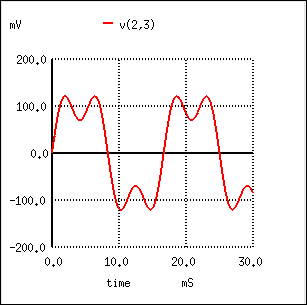
Well I gave given this much thought. I found inspiration in the Timex/Sinclair official ZX81 extended clone the TS1500. It had an improved cassette interface, and yes, it was using a transistor, but just slightly different than my first transistorized attempt. There were some doubts about the values used, so I plugged the schematic into LTSpice, the Analog design simulator of Linear Technology, which is free to download and use. and this is what I came up with after intensive value tweaking:

This seemed to work very well, but in fact I saw that when I used a longer sequence of bursts C1 charged up, and after the last pulse the output level did not return to zero immediately, so I increased C1 to 10uF, its possible that lowering C1 would have also worked, but it would probably have made the circuit less sensitive. Also, putting an 1K terminating resistor on the input also helped with the same problem, and it would also be a good idea to put a small cap over the input to reject HF pulses. In any case this is what the simulator thought that would happen when a stream of eight pulses would be presented at the output, followed by silence:

As can be seen the output are eight positive going pulses, all the way from ground to 5Volt, with an immediate return to 0V afterwards, exactly what we need. The ZX81 cassette interface uses four pulses for a zero, and eight pulses for a one, each pulse is 150 uS on, and 150 uS off, so lasts 300 uS, between each pulse is a 1300 uS interval where the signal should be low. The cassette interface makes one "swing" from every pulse the ZX81 generates, so it makes no difference whether you detect the negative going, or the positive going part of the "swing"

So my solution uses the negative part of each "swing", but that makes no difference.
One advantage of this input circuit is that it works with modern CMOS logic (the original ZX81 used an LS TTL compatible input for the cassette input, and because of it the input circuit could be incredibly simple, even if it needed a lot of signal to work. My circuit generates pulses compatible with any kind of (5V) logic, and is much more sensitive than the original, at least that was the theory....
So yes, I built a prototype and tried it, with success! I was given a wave file by a ZX81 enthusiast, witch a small ZX81 recording, and it worked fine!
I'm still looking for a player that can convert ".P" recording files (for emulators) to sounds output from a laptop (or tablet), so I can load games and such.
I also need to test the cassette output system, and patch this interface into my prototype, as keeping the small perfboard permanently attached to my prototype is not an option.
Updated schematic of ZX81+35 here, and implemented layout changes. This is the new layout:

March 28, 2016 improved the cassette interface
Even though I loaded a small program successfully, I was still concerned that the interface stopped working when I input a louder signal, while my LTSPICE model did not suffer from the same problem. so "a little bird" told me I should investigate the problem further, and that the problem could lie in the "long term" behaviour of the circuit. With my intuitive grasp of what needed to happen to fully understand that behaviour,I started working on a SPICE model that more fully would imitate the (average) behaviour of the ZX81 cassette signal. Generating a fully compatible signal with LT Spice would be very difficult, but by generating a sine with 300 uS intervals, and shorting it to GND with multiples of that same interval I should be able to generate a very similar signal. So I went on to wrestle with the "switch" functionality of LTSPICE. After I had that working I decided to generate six cycles of the sine wave, followed by four cycles (1200 uS) of shorting the signal to ground. this lead to a stream of six 300uS pulses interspersed with 1200 uS of silence. This lead me to the discovery of the problem, that the "DC level" over a longer period started to "creep up", so after a few hundred uS the pause level between two bits became a logical high, instead of a logical zero, This will badly corrupt the loading process, see this picture:

The reason was obviously that the 10uF capacitor slowly started charging up (the red line). The solution would be to decrease the value of that cap, enough so that it would discharge in the time between two pulses, and further discharge in the 1300uS between two bits. A circa 80K discharge path was already provided through resistors R79, R58, and R59, [5], or R6, R1, and R3 in the SPICE diagram below
After some time of experimenting with capacitor values, and audio input levels, (higher levels would widen the pulse width of especially the last pulse) I decided that 4n7 was the optimal value, 1nF would make the circuit almost insensitive, and 10nF would make the last pulse excessively wide.
This is picture of the LTSPICE set-up, and the waveform of the pulses after 150mS.

The "little bird" now tells me that this circuit should work fine, and it should also work with "turbo load circuits". I found several upload programs that can "play" .P files, one of which that uses a turbo load concept, I will patch my ZX81+35 prototype, and try to load some more files, until I'm satisfied the cassette interface works okay. Then I will try creating saving files to an audio recorder, and loading these recordings back. Note the choice for six pulses is an attempt to simulate an average of 4-pulse and 9-pulse streams, so its not an error. The layout has not changed from the previous situation with a 10uF cap.
March 29 Cassette loading works fine!
I can Confirm that loading even longer programs works fine. If you set the volume a bit louder you can also load files in a propriety turbo charging format. Next up saving files. I will also try running some variations of high-resolution software to see just how compatible my ZX81 clone is.
1/4/2016 ( = 4^0 / 4^1 / 4^2 ) Updated 3D preview
In preparation of the design for (the 3D rendering of) an enclosure I updated the preview ( done with Altiums 3D rendering ). The corrections are a better proportion of the PCB, (previous previews did not have the exact 10 x 10cm dimension of the real boards, (but more 9.2mm high by 10mm wide), the current preview corrects that. The preview now also uses realistic male/female angled pinheaders for the interconnect between keyboard and PCB, (so the outer dimensions of the enclosure are now known) the size of the expansion board was adjusted so it uses the available space more effectively, and planned mounting holes were added to mount PCB, expansion board and keyboard to the bottom halve of the planned enclosure. I will get my inspiration from the QL. the updated preview replaces the previous rev 2.0 preview, and page header and project thumbnail pictures. in time I will design 3D rendering of the two "clam shell" halves so you can get an impression of how the ZX81+35 would look in its enclosure.
April 3, 2016 found, and solved, a "pulse splitting" problem in the cassette interface
Found a problem in the cassette interface and solved it. When I looked at the digital playback signal, with a digital oscilloscope, and compared it with the input signal I found that my playback signal did not look nice and clean, but seemed to have a lot of odd harmonics in it which deformed the signal so much that the "top op each pulse had a big dent in it", like in this picture:
https://www.ibiblio.org/kuphaldt/electricCircuits/AC/22042.png
I also saw that the interface was often splitting this signal into two separate pulses. Using LTSPICE, I added a first odd harmonic to the signal, and so managed to re-create the signal I saw, which I fed to the interface. And I could indeed observe how the signal was split into two pulses, amazingly the ZX81 (clone) could still load the file! It seems (from interpreting the Z80 code) that the ZX81 does not count the number of pulses in a burst, but merely counts the total high time to determine if a 0 or 1 was sent, so its more or less impervious to this problem, which doesn't mean I don't want to solve it! So I tweaked the circuit to see if I could make it less sensitive to signals "with a dent in it", after a lot of experimenting, (I had not much faith I would succeed) I found that the amazingly simple solution was to increase R59 from 4K7 to 10K, bravo for LTSPICE! So I made that change on my prototype, and indeed loading became more reliable. So I updated the schematic. In fact I'm still not completely satisfied with it, but further improvements would involve adding (zero crossing) analog logic, a comparator or opamp circuit. It could be that such a circuit is in the ULA of the ZX81, but I doubt it, at least in the ZX80 the signal was input directly into a LS367 buffer input. For a moment I considered simply replacing the circuit with a single gate LS type buffer, but I would get the same notorious insensitive audio input that the original ZX81 had, so thanks but no thanks!
The schematic (.PDF) is again updated.
Started design of an enclosure for the ZX81+35
I used my 3D preview in Altiums 3 modelling to start the design of an enclosure. The enclosure will measure about 185 x 185 mm and will be about 30mm high. Here is a preview of it:

The enclosure will be black (What else?) but this preview has different parts in a different color (scale of grey) the bottom plate is grey, raised round posts for screwing the two parts together are light grey, except the raised post for screwing the main PCB to the bottom, which is green. the sides are black, the semitransparent keyboard overlay is white, and will actually be part of the top halve of the enclosure. The plan is to make the grey bottom plate out of laser cut wood, and the rest out of 3D printed plastic, The result will look something like this:

nice no? The top halve will complete it, and will make it resemble the original ZX81 quite nicely, But with a more Sinclair Spectrum 2+/QL kind of look (flat top). Its dimensions will also be in the exact same ballpark as the ZX81, just about 10% bigger.
This is how I envision what a ZX81+35 expansion board should look like
Here is a picture of my (pie in the sky) idea on how a typical expansion board could look like. This one creates a ZON-X compatible sound card, and uses its GPIO's to interface to an µSD-card. It also shows how a ZX81 compatible edge connector can be implemented (it could be an otherwise empty extension board).

On april 12, 2016 I was diagnosed with Sleep Apnea, which means I cannot drive a car!
This means I will have very limited access to RevSpace :-( The good new is that I now know that I have Sleep Apnea (Apneu in Dutch) which means that I have over 30 breathing stops per hour in my sleep each night, which nearly wake me up. Its the reason for being tired all the time, and for my subconscious fear of going to bed which has lead to a very strange biorhythm. Also good news is that apnea is treatable, with an overpressure (APAP) device I will need to wear in my sleep, I will get a test for one next week (normally it takes over a week, so I'm lucky). Id did a sleepover at MCH and can say the APAP device worked very well for me, I will be offered one in two to three weeks time, I can't wait! If I used it for 2 months and it works well, I will get my permission to drive back.
https://en.wikipedia.org/wiki/Sleep_apnea
for now I need to use public transport, which luckily in the Netherlands is quite good. Every 15 minutes I can travel to my work by train, in about 50 minutes, with just one transfer stop. I was not aware public transfer would be this good. and there are also several bus routes to my work, but they are a bit more complicated. Unfortunately the Spoorlaan, where the building of RevSpace resides, isn't easily accessible by public transportation, there are no bus-stops nearby, meaning a 30 minute walk is imperative, or perhaps a bike ride is needed, taking a bike on the train to work is possible, but cumbersome.
I bought a backpack, with a laptop compartment, So I can take a bike from station Voorhof to RevSpace, I will attempt the trip today, Sunday May 1 to bring my laptop and stuff to RevSpace.
I continued designing for the ZX81+35
I now have used my folding bike a couple of times to reach RevSpace, and have started on an (example) extension board. This one will carry a sound chip, (PSG) of the AY-3-89xx family, I'm planning to use the AY-3-8912 which is still for sale on e-bay. It will have its own 3.84 MHz clock, as the clock of the ZX81+35 could vary, and it will probably have a divide by 32 or 2 (jumper able) after it to generate the PSG clock. I 'm initially planning to be compatible (I/O address) with the original (ZON X81) PSG for the ZX81, but with the addition to be able to read from the PSG chip, not for joysticks (an often used use for the GPIO's of the PSG) but an attempt to create an (bit banged ) SPI interface, so I can add either an EEPROM or even a (simple) SD-CARD interface, we will have to see how well that goes, I have to experiment with the capabilities of the PSG's GPIO port.
Okay, and the expansion board will add a standard ZX81 expansion port edge connector, so you can connect a ZX81 printer, among other things.
17 May, 2016 Started with PSG expansion board
I tried to design a schematic of the original Zon-81 before creating my own compatible version. A first (unfinished) version of the schematic can be found here: File:Sound expansion (preliminary).pdf
second version updated on may 24, 2016.
-1.png)
Third version: updated on June 7, 2015
Started design of my own PSG board
Its development is described in its own article here https://revspace.nl/Zon_X-81_Programmable_Sound_Generator_expansion_for_ZX81PLUS35
Found basic, but major error in ZX81+35 Updating to rev 4.0
While designing the PSG expansion board I look once again to the expansion port and made a discovery that made me say some expletives &*$$$#)**^& ! I've made a mistake in the very beginning about the orientation of the expansion connector, such that it is now upside-down to how it should have been. This error is expressed in how the expansion connector was drawn in the schematics, (which probably explains the origin of the error) with pin 1 on top, and pin 23 on the bottom, but the edge connector should have been just rotated 90 degrees clockwise, which means pin 1 should have been on the bottom, not on the top, that is, If I wanted to be compatible with a real ZX81, which I do!!
This means a very large layout modification is necessary to accomplish this. I could have "fixed" it by rotating the pins on the PSG board, but in my opinion that is cheating. Its a genuine error and has to be fixed!
So I started by modifying the schematic, so it corresponds with how it should be laid out. this is the new schematic, I consider the change big enough to warrant updating to revision 4.0: File:ZX81plus35 REV 4.0.pdf
I have also started on the re-layout work. Now done three evenings of layout edits, during my vacation, but its September already and it's still not finished, its proven to be really difficult, hold on will need a couple of Thursday evenings more....
also thinking about a trick to keep video stable in turbo mode, it seems the trick is to lower the clock at the very start of each video line, during the line counter reset, that should be doable. But I still must test if that works. The layout edits now also include that the edge connector clock is a steady 3.25MHz clock, and NOT the CPU clock, so PSG should be able to work in turbo mode.
p.s, forgot to tell you all that for some months now I have re-gained the right to drive, the CPAP machine does its work fine, APNEA incidents dropped from 30 per hour to less than two! so getting much better sleep now.
13 September 2016 Reached 100% connectivity
Well, I finally managed to re-layout all connections. its still a bit of a mess, so I have to error check and optimize it, but at least it seems possible to lay-out it (unless the design contains an error I cannot solve, but that is a -very- slim chance). Next week I should be able to finish it.
20 September 2016 Revision 4.0 is ready
Finished the layout for revision 4.0, The new layout is fully checked and optimized. Here is a picture of the new layout.

As you can see this is a quite large change. Specifically in the top left quarter.
I will now continue with my sound expansion card design, which also needs to flip the edge connector orientations so the pin 1 of the pinheader connectors and edge connector are at the "bottom".
1 November 2016, website problem
This website has developed a problem; redirects with "+" sign in the filename no longer work! I have replaced the latest pictures and .PDF files with ones that use "plus" instead of the + character. The web master is aware of the problem, and he has renamed a few pages, so you can at least visit my two projects that had a + in the filename. Hopefully the problem will be resolved soon, probably by replacing each "+" in an URL to a .PDF by "plus". On November 3 I managed to change the filenames pointing to .PDF's (and a few other non picture formats) in this and the other affected pages to versions with "plus" instead of "+", in the hope that the webmaster will come through with his promise to do the same for these files, so the pointers do point to a valid location once more. doing that to URL's pointing to .PNG pictures might be trickier as changing the URL may delete the picture itself in this thread, until the pictures URL is also changed. So for now I only replaced URL's not used in pictures. until i'm informed the pictures are copied to ones using "plus" instead of "+" in their filename. There was also the case of another page like this, (https://revspace.nl/Zx81plus34) a predecessor of this page talking about why I wanted to create the ZX81 clone that could not be accessed because it also had a "+" in the file name, but I managed to copy it to a new version with plus in the file name instead of + without help from the web master, its here [6]
29 November 2016, website problem mostly solved
I managed to find replacements for all the .PDF's and a few .ODF (BOM's) in this thread, and uploaded them with filenames without using the + sign There will be a few pictures on this page that when clicked upon will give a redirect error, but I hope that won't be a problem.
2017 has arrived
Its now 2017, and Revspace has just moved to a new location, and I feel my ZX81+35clone is almost finished, but not yet completely. Thought about updating the name to ZX81+36, but rejected it (for now). There is one last Issue I would like to solve, and that is to get turbo working, without the screen shake that it has now. I fear that the problem is in the mechanism that switches the clock from turbo to normal when a screen has to be drawn, it seems the moment between the horizontal sync pulse and when characters are started to be clocked out is affected by when the mechanism decides to run in turbo mode, and when not. The solution it seems is to switch turbo off during the whole period of generating the screen, and only turn it on during the vertical sync period. I still have to decide how to do that, it will take some experimenting. I hope to finish the ZX81+35 after my intermittent projects have finished. Hopefully I will also be able to test my PSG board with it before I release the design, but testing it is made more difficult with my old (second) prototype because the expansion header has rotated 180 degrees. I also have to make a prototype board of the PSG to do that.
Its 2019 and I have decided to release my ZX81+35
Even through I never got turbo mode (clock speed doubling) to fully working, as a ZX81 clone ZX81+35 works more than fine, and there seems to be some interest in it, so I released it under a BSD-3 licence (free to use and copy for non commercial use).
You can find all the files you need to build your own version on GitHub here: https://github.com/mahjongg2/ZX81plus35
it now includes:
- Schematic for revision 4.0 (the latest version) as a .PDF (File:ZX81plus35 REV 4.0.pdf)
- Bill of materials (updated to the latest version) as .ODS (spreadsheet)
- Ulticap and ultiboard files of the schematic and layout (CAD files)
- production files (gerbera and drill files for revision 4.0) you can upload to any PCB manufacturer to get your own PCB (only main PCB, for now, not keyboard PCB, but you can hand build one with perfboard)
- previews of the Top and bottom of the revision 4.0 PCB, so you can see what the PCB should look like.
- keyboard overlay as .PDF (original version) you can plasticise it, and stick it over your keyboard.
to come (I'm working on it):
- Keyboard PCB layout
I have also released prototype schematics and layout of my ZON compatible expansion board for a programmable sound chip on another GitHub page named "PSG-for-ZX81plus35-ZX81-clone". this expansion board adds AY-#-8912 sound generation, and a SD-Card slot through the PSG's expansion ports. This PSG board should be compatible with software for the ZON board for the ZX81, such as the dancing demon program, and some others, and can be used to create "chiptunes". It also serves as an expansion interface so you can use ZX81 peripherals that use an edge connector (the board brings out a real ZX81 edge connector), and can be used as an example how to add peripherals to my ZX81 clone. Note that I never had the chance to test it with older versions of my ZX81+35, as it needs the corrected expansion bus, (that only revision 4.0 has) and I never built the revision 4 version.
So this expansion board has not been tested by me, but I believe it is correct, feedback if you do test it is appreciated (use the thread in the off-topic section of the raspberry PI foundation, or e-mail me at mahjongg at xs4all.nl
August 22, 2019 Started on the Keyboard PCB, compatible with the keyboard overlay
Although I designed the schematic (using UltiCap) and build a working prototype on Perfboard, I never did finish a real PCB for it. I will design one using KiCad, no way I'm going back to my old windows laptop, and try to use UltiCap and UltiBoard again. I want to retire that laptop forever.
So here is the schematic for a Keyboard PCB compatible with the ZX-81+35, meaning that the order of the data and address wires is correct, and other pinheader positions are correct. For example the three pins for LED's are in-between the data and address headers. In this case the 18-wires are in the order nRESET, RESET-GND, KD4, KD3, KD2, KD1, KD0, POWER-LED, TURBO-LED, LED-GND, KA11, KA10, KA12, KA9, KA13, KA8, KA14 and KA15.
The keyboard PCB can be connected to the ZX81+35 through a piece of 20-way flat flex cable with wire ends (https://nl.farnell.com/te-connectivity/fst-22a-20/ribbon-cable-ptfe-20way-2/dp/1310356), with 2 wires removed, soldered to the keyboard PCB on one end, and stuck into an 18-pole female socket on the main PCB.
The schematic of the keyboard has been thoroughly researched so that I'm sure it will be compatible with both my clone, and with a real ZX-81.
There seem to be some differences in the order of keyboard connections between a ZX-81, and a Spectrum, which confuses things. it seems that compared to the ZX-81 Spectrum keyboard wiring has KA9 and KA12 swapped. Note that in the ZX-81 the PCB seems mounted upside down, but this is actually an optical illusion because the PCB is mounted to the TOP case half, not the bottom half, so keyboard and PCB have the exact same orientation, just like my own design).
I will do extra checks to make sure my wiring order is correct, for that I have arranged a real ZX-81 (plus memotech memory extension) to do extra compatibility checks, and check some dimensions, such as the keyboard recess, which I could not find online.
My prototype keyboard had roughly the same size as the original, although a tiny bit larger, but now I have designed the keyboard PCB so that its outer dimensions are such that it exactly fits inside the recess of a real ZX-81, (after you round off the PCB corners a bit with a file) and its flat wire connection should fit exactly through the slit in the real ZX-81 enclosure. This means the PCB is 2.5 inch high, and 6.2 inch wide, this is a preview of the placement, of the buttons, and connectors, and the PCB size. File:ZX-81 Keyboard-F.SilkS.pdf
Its probable that the buttons in this layout will move a bit up, to make place for 5 wires of Data wiring underneath. the full PCB has not yet been routed, but I foresee this will be necessary.
The reset can be a simple push button mounted on the side (or back) of the enclosure.
The carefully checked keyboard schematic for the ZX81plus35 is here:
File:ZX-81plus35 Keyboard.pdf
and this is a picture of this .PDF:

The keyboard uses forty 6 x 6 mm buttons ( MCDTS6-2N or equivalent ) with a 6.5 mm x 4.5mm pad pitch (long ends connected) with about 0.9mm thick pins (hole size of PCB = 1.1mm). These are very common. Make sure you use keys with a reasonable long stem, so they stick out well above the keyboard template. The stem width should be about 3.5mm, and the stem should be round.
For connection to a real ZX-81 you can use a piece of FST-22A-15 flat flex cable with wire ends, (https://nl.farnell.com/te-connectivity/fst-22a-15/ribbon-cable-ptfe-15way-2/dp/1310375 ) cut into 5 wire and 8 wire parts, soldered to the underside of the PCB. The PCB can then be mounted to the plastic case. After removing the old foil keyboard, and sticking the FST-22A cable ends through the opening in the case, the PCB can then be screwed to the case with four 2.5mm self tapping plastic screws, after drilling four small 1.5mm holes in the case. the other ends of the flat-flex cables should fit into the sockets on the zx-81 main board.
If you don't want to use the expensive FST-22A cable, its also possible to solder wire ends to cheap standard flat-flex foil cables, (https://nl.farnell.com/c/cable-wire-cable-assemblies/cable-assemblies/ffc-fpc-flat-flex-jumper-cables?searchref=searchlookahead) and solder the wire ends to the keyboard. If you first stick the flex-foils into the connectors, so their orientation is such that they make contact with the connectors, one being 180 degrees rotated relative to the other.
September 2, 2019 Made a new component overview (assembly drawing) for rev 4.0

September 11, 2019 Keyboard ZX81+35 PCB finished
Will save the files to GitHub, but here is a preview:

I managed to design it on a single sided PCB, using the fact that pairs pins of the switch over the long size are connected together, so can be used as wire bridges.
This is how the component-side of the PCB will look, note there is no solder mask (green lacquer) layer, but it does have a white silkscreen (text print).

and this is the solder side (mirrored) with soldermask.

I'm considering designing a simplified (to build) version, based on an ULA replicate
The current ZX81+35 design is nice, but has a few deficits that make it difficult to build, as a kit. I'm considering to simplify the build, by designing a ULA replacement, based on an FPGA with my ULA replacement logic in it, and also to build a replica ZX-81 clone for it which has only (a small amount of) PTH components on it, very similar to the original ZX-81 kit. It will be a more classical design, looking more like a real ZX-81 in size and shape, not restricted to a 10x10cm PCB, with (expansion) connectors in roughly the original locations, no need to worry too much about the infamous "wobble problem" with 32K of RAM (LY62256) on board, so returning to an edge connector in the back, and also with an 8K Byte FLASH ROM in a DIP package as PCB space is no longer a premium.
The main job this time will be to replicate the original ULA, I'm planning to create one that will also work in a real ZX-81, so it will be a small QPF on a 40-pin carrier board, this will be a separate project.
This time it will be done in KICad. watch this space.
p.s. This idea never happened instead I simplified the plus35 by creating the plus38, which only uses pin through hole (PTH) technology, and leaves out all the stuff not necessary for a ZX-81 clone, and uses a PCB that is size and drill hole compatible with a real ZX-81.
If you have build a ZX81+35 and have a problem, you can reach me here
I have gotten reports about a person who has built my ZX81+35, and needed help solving a (minor) problem, and I realised I have given no address where you can reach me if you have a problem building my clone.
You can reach me at ,mahjongg commercial-at xs4all.nl, (no need to publish my full e-mail address for mail address scanners to find). obviously I will be happy to give you free advice on how to find a problem, and might also offer free repairs, within reason (for example I Won't "repair" a ZX81+35 that has been powered with 12V) LOL.
Someone attended me that the component overview drawing contains an error. U13 is listed as a 74HC32, while in fact its a 74HC00. Also there is a problem with downloading the BOM spreadsheet. Both problems are now fixed.
October 21, 2016 Received a free built ZX81+35 and its working
I only had to build an adapter for my keyboard, as I still wanted to keep it working for my own Revision 2.0 copy, but revision 2 uses the old wiring scheme.

This is a program I tested it with:
10 FOR X = 0 TO 255
20 PRINT CHR$ X;
30 NEXT X
and this is the resulting output, it is simply perfect, all characters fit perfectly together, and are clean and sharp:

I found one small error while testing board, a text printed on the PCB near the turbo switch was wrong! sliding the switch to the left sets it in turbo mode, and to right in normal mode, but the text on the PCB claims that left is normal mode, and right is turbo mode. I would suggest disabling turbo mode, by wiring the switch position permanently to the right. Meantime a new silk screen file was created and updated in the GitHub production files .ZIP. The component overview drawing has also been corrected, and now shows default jmper positions. in turbo mode the display becomes unstable and jumps from left to right during printing. I could do a new attempt to find the cause. I can also try a patch to generate loading bars during a cassette load.
June 2020 I received news about errors in the latest gerber files
There seems to be slipped in a wrong file among the gerber files I uploaded in October 2020, it seems the top solder mask layer was a wrong one, and did not belong in the .ZIP file I uploaded to Github. when I downloaded the gerber files myself I could see there was something wrong, especially in the top right hand corner.
These picture shows screenshots of the gerber files I downloaded from GitHub end June, 2020, left the full picture right details showing errors in the soldermasking.
a.o. Missing pads for C26 and R70 so this is the old rev 4,0 version, don't use this to create PCB's!


Because of the corona lockdown, which also affected RevSpace, It took me some time to investigate the problem, also because I needed an old, and previously written off laptop, that has no battery and a French keyboard, but it has the now defunct CAD software with which I designed the ZX81+35.
For the new ZX-81+38 I bought a new Laptop, and switched to KiCAD, and I hoped I would never have to use the old beast again.
But I decided the only way to solve the problem reliably was to get the old laptop back and get it to work again, and create a completely new set of corrected gerber and drill files revision 4,1
So these are pictures of the gerber viewer showing rev 4,1


I visually checked if these gerber files are identical to the known good previous build of the revision 4.0 of august 2019, which I know is working well
I have uploaded the Gerber files, and also a Rev 4,1 Schematic (for completeness as its identical to the rev 4.0 one) to GitHub
If you want the latest schematic, here it is: File:ZX81+35 REV 4.1 schematic.pdf
May 16, 2022 Yes after the two year long corona crisis has happened I'm back
I have good news, I just found out that an anonymous german ZX-81 enthusiast, I will call Thomas, has built this ZX-81 clone, but not only that, but he also built the PSG. He got everything working, including getting sound with the dancing demo "game", but not only that! He thought he could get the SD-Card interface working, an idea I gave up on because I could find no way to de-select the SD-Card (the chip-select /CS signal going to the SD card) while switching from a read to a write mode and back. If I tried to do that the SD-card would be de-selected, and so driving the SD-card seemed impossible, and I gave up on this idea, but Thomas not only found a way to circumvent the problem, he actually got the SD-Card interface working with minor patches, so he designed and implemented the patches, but also wrote the firmware to drive SD-Card reading, and wrote an menu driven user interface! To make using the card easy he stored his code in a 8K ROM expansion, so he patched the ZX81+35 so it would support 16K ROM. Because an SD-Card interface that only works when you load firmware from tape is not worth much! Actually the sd-card is at least ten times faster than loading from tape, and is much more convenient as you have a menu to choose a game from. see more here:https://revspace.nl/Zon_ZX-81_Programmable_Sound_Generator_expansion_for_ZX81PLUS35#15_march_2022.2C_great_news_a_PSG_board_builder_has_gotten_the_SD-card_interface_working and here (Im planning a version for real ZX-81's and my other clone the zx81+38 https://revspace.nl/Zon_ZX-81_compatible_PSG_%2B_32K_RAM_and_SD-Card_interface_expansion_for_ZX-81_and_clones
Well this is such a great development that I have decided to make it official, so I will design new versions of the ZX81+35 (for extra 8K ROM support) and a new version of the PSG board, with his patches.
keep watching here, and the PSG project page, for updates...
May 21, 2022 revision 4.2 supports 16K ROM space, and corrects some errors
I Updated the schematic and layout with revision 4.2, which now will support a (default) ROM space of 16K instead of the previous 8K, so you can put 16 K of code into the flash ROM chip, instead of the previous 8K, The new 8K extension can be used to place the firmware for SD-Card support in, so you can run the SD-card menu system without having to load anything from tape when using my programmable sound card AY-3-8912 ZON-ZX81 PSG card with a SD-Card reader built in. Also I repaired a hardware bug, Address lines A13 and A14 were erroneously swapped in revision 4.1, that is now corrected, also changed (although I would not call it a correction) is that now the expansion port uses the same clock signal "0" as the CPU, that is it will now chance clock speed with turbo mode turned on, but note that turbo mode is still not working correctly with video generation, its advised not to use turbo mode anyway, unless you only use FAST mode.
The new schematic (In colour) is here:
File:ZX81+35 REV 4.2. schematic color.pdf
I also finished the new Layout, here is a preview of it:
File:ZX81+35 REV 4.2 layout preview.PDF
You can use the older placement diagrams as (except for the 8K/16K ROM patch resistors below U23) the component placement has not changed. see: https://revspace.nl/File:ZX81plus35_silkscreen_overview_rev4.png
I will upload Gerber and drill PCB production files on my MAHJONGG2 GitHub pages soon: